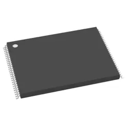
画像は参照用のみです。
XCZU15EG-L1FFVB1156I
IC SOC CORTEX-A53 1156FCBGA
- メーカー
- Mfr。パート #XCZU15EG-L1FFVB1156I
- パッケージ FCBGA-1156
- データシート
- 在庫中2195
100% オリジナル &新しい
出荷の準備ができている24時間
365日の保証
RFQおよびもっと割引を得る
仕様
| Package | Tray |
| Series | Zynq® UltraScale+™ MPSoC EG |
| ProductStatus | Active |
| Architecture | MCU, FPGA |
| CoreProcessor | Quad ARM® Cortex®-A53 MPCore™ with CoreSight™, Dual ARM®Cortex™-R5 with CoreSight™, ARM Mali™-400 MP2 |
| RAMSize | 256KB |
| Peripherals | DMA, WDT |
| Connectivity | CANbus, EBI/EMI, Ethernet, I²C, MMC/SD/SDIO, SPI, UART/USART, USB OTG |
| Speed | 500MHz, 600MHz, 1.2GHz |
| PrimaryAttributes | Zynq®UltraScale+™ FPGA, 747K+ Logic Cells |
| OperatingTemperature | -40°C ~ 100°C (TJ) |
| Package/Case | 1156-BBGA, FCBGA |
概要
Description
The XCZU15EG-L1FFVB1156I is a high-performance System-on-Chip (SoC) from Xilinx's Zynq UltraScale+ MPSoC family. It integrates a quad-core ARM Cortex-A53 processor with a dual-core ARM Cortex-R5 real-time processor and programmable logic, allowing for flexible and efficient processing capabilities.
Key features include:
1. Processing Power: The ARM Cortex-A53 cores are designed for high-performance applications, while the Cortex-R5 cores excel in real-time processing tasks.
2. FPGA Fabric: It includes a significant amount of programmable logic, enabling custom hardware acceleration and parallel processing for specific applications.
3. Connectivity: The SoC supports various communication interfaces, including PCIe, Ethernet, and USB, making it suitable for a wide range of applications.
4. Applications: Commonly used in embedded systems, industrial automation, automotive, and data acquisition applications due to its versatility and performance.
This device is ideal for developers looking to leverage both processing and hardware customization in a single platform.
Features
The XCZU15EG-L1FFVB1156I is a SoC (System on Chip) from Xilinx's Zynq UltraScale+ family. Key features include:
1. Architecture: Combines a quad-core ARM Cortex-A53 processor with a dual-core ARM Cortex-R5 real-time processor and programmable logic (FPGA).
2. Performance: Offers high-performance processing capabilities with a maximum clock frequency of up to 1.5 GHz.
3. Logic Cells: Contains over 15,000 logic cells, enabling complex designs.
4. Memory: Supports up to 4MB of on-chip SRAM and integrates various memory interfaces, including DDR4 and LPDDR4.
5. I/O Options: Features a range of I/O standards and interfaces, including USB, PCIe, and Ethernet.
6. Power Efficiency: Designed for low power consumption while delivering high performance, suitable for embedded applications.
7. Development Tools: Compatible with Xilinx Vivado Design Suite and Vitis for streamlined development.
This SoC is ideal for applications in automotive, industrial, and communication sectors.
Package
The XCZU15EG-L1FFVB1156I is packaged in a FFG (Fine Pitch Ball Grid Array) package type. This specific package has 1156 balls and is designed for high-performance applications, offering efficient thermal and electrical characteristics.
Pinout
The XCZU15EG-L1FFVB1156I is a member of the Xilinx Zynq UltraScale+ MPSoC family. It features a total pin count of 1156.
This device integrates a powerful combination of Processing System (PS) and Programmable Logic (PL), making it suitable for a variety of applications including embedded processing, signal processing, and high-performance computing. The device includes ARM Cortex-A53 and Cortex-R5 cores, along with a range of interfaces for connectivity, such as PCIe, USB, and Ethernet.
Additionally, it supports various I/O configurations, including high-speed transceivers, GPIOs, and memory interfaces, enabling it to connect with a diverse array of peripherals and systems. The Zynq UltraScale+ architecture allows for significant flexibility and scalability in design, catering to both consumer and industrial applications.
Manufacturer
The XCZU15EG-L1FFVB1156I is manufactured by Xilinx, Inc., which is a leading company in the field of programmable logic devices and FPGAs (Field Programmable Gate Arrays). Xilinx specializes in advanced semiconductor technology, offering products that support a wide range of applications, including telecommunications, automotive, aerospace, and industrial automation.
The XCZU15EG is part of the Zynq UltraScale+ family, which integrates a processing system with programmable logic, allowing for high performance and flexibility in system design. Xilinx is known for its innovation in reconfigurable computing and has a strong focus on enabling engineers to create complex, customizable solutions. In 2020, Xilinx was acquired by AMD (Advanced Micro Devices), further expanding its capabilities and resources in the semiconductor market.
The XCZU15EG is part of the Zynq UltraScale+ family, which integrates a processing system with programmable logic, allowing for high performance and flexibility in system design. Xilinx is known for its innovation in reconfigurable computing and has a strong focus on enabling engineers to create complex, customizable solutions. In 2020, Xilinx was acquired by AMD (Advanced Micro Devices), further expanding its capabilities and resources in the semiconductor market.
Application
The XCZU15EG-L1FFVB1156I is a versatile System on Chip (SoC) from Xilinx's Zynq UltraScale+ series, suitable for various applications, including industrial automation, robotics, automotive, telecommunications, medical imaging, and machine learning. Its combination of programmable logic and ARM processing capabilities enables performance optimization in real-time data processing, high-speed communication, and complex algorithm execution across diverse sectors.
Equivalent
The XCZU15EG-L1FFVB1156I chip is part of Xilinx's Zynq UltraScale+ MPSoC family. Equivalent products include the XCZU9EG, XCZU13EG, and other Zynq UltraScale+ models with similar specifications but varying resources, performance, and power characteristics. For specific applications, check the individual datasheets for exact feature comparisons.
出荷
出荷方法私たち
DHL、FedEx、TNT、UPS、またはあなたの選択の他の運送業者を通じてグローバルな出荷サービスを提供します。
出荷料参照(DHL/FedEx):
DHL の: 配送費は25ドル〜45ドル(0.5kg)の範囲で、推定配送時間は2〜5営業日です。
フェデックス: 配送費は25ドル〜40ドル(0.5kg)の範囲で、推定配送時間は3〜7営業日。
UPS の: 配送費は25ドル〜45ドル(0.5kg)の範囲で、推定配送時間は3〜7営業日。
TNT社: 配送費は25ドル〜65ドル(0.5kg)の範囲で、推定配送時間は3〜7営業日。
EMS: 配送料金は30〜50ドル(0.5kg)の範囲で、推定配送時間は7〜15営業日です。
登録航空郵便: 配送費は2〜4ドル(0.1kg)で、推定配送時間は5〜20営業日です。
支払い
Payment Methods
支払い期間は100%前払いです。
現在、下記の支払い方法のみを受け入れています。:
1. ペイパル
2. クレジット・デビットカード
3. ワイヤー 転送
類似
-
![MX25L3233FZBI-08Q]() MX25L3233FZBI-08Q
Macronix
-
![MX25V1635FZNQ03]() MX25V1635FZNQ03
Macronix
-
![MX25V4035FZUI]() MX25V4035FZUI
Macronix
-
![MX25V2033FM1I]() MX25V2033FM1I
Macronix
-
![MX25R3235FZNIL0]() MX25R3235FZNIL0
Macronix
-
![MX30LF2G28AD-TI]() MX30LF2G28AD-TI
Macronix
-
![MX25L8035EM2I-10G]() MX25L8035EM2I-10G
Macronix
-
![MX29GL512FHXFI-11G]() MX29GL512FHXFI-11..
Macronix
-
![MX25L12833FZ2I-10G]() MX25L12833FZ2I-10..
Macronix
-
![MX25U25645GXDI00]() MX25U25645GXDI00
Macronix
-
![MX29LV160DTTI-70G]() MX29LV160DTTI-70G
Macronix
-
![MX30LF4G18AC-TI]() MX30LF4G18AC-TI
Macronix