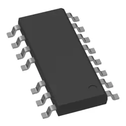
画像は参照用のみです。
XCVU37P-2FSVH2892E
IC FPGA 624 I/O 2892FCBGA
- メーカー
- Mfr。パート #XCVU37P-2FSVH2892E
- パッケージ FCBGA-2892
- データシート
- 在庫中6485
100% オリジナル &新しい
出荷の準備ができている24時間
365日の保証
RFQおよびもっと割引を得る
仕様
| Package | Tray |
| Series | Virtex® UltraScale+™ |
| ProductStatus | Active |
| NumberofLABs/CLBs | 162960 |
| NumberofLogicElements/Cells | 2851800 |
| TotalRAMBits | 74344038 |
| NumberofI/O | 624 |
| Voltage-Supply | 0.825V ~ 0.876V |
| MountingType | Surface Mount |
| OperatingTemperature | 0°C ~ 100°C (TJ) |
| Package/Case | 2892-BBGA, FCBGA |
概要
Description
The XCVU37P-2FSVH2892E is a high-performance FPGA (Field-Programmable Gate Array) from Xilinx's Versal UltraScale+ series. It is designed for a wide range of applications, including data center acceleration, telecommunications, automotive, and industrial automation. This FPGA features a large number of logic cells, high-speed transceivers, and advanced processing capabilities, allowing for parallel processing and real-time data handling.
The "XCVU" denotes its family, while "37P" indicates its specific variant. The "2FSVH" denotes the package type and speed grade, and "2892E" refers to the pin count and temperature range. The device supports multiple programming models, including VHDL, Verilog, and high-level synthesis (HLS) for ease of development.
Key features include integrated AI engines, DSP slices for signal processing, and support for various connectivity options like PCIe and Ethernet. The XCVU37P is particularly suited for applications requiring high throughput, low latency, and adaptability to changing workloads.
The "XCVU" denotes its family, while "37P" indicates its specific variant. The "2FSVH" denotes the package type and speed grade, and "2892E" refers to the pin count and temperature range. The device supports multiple programming models, including VHDL, Verilog, and high-level synthesis (HLS) for ease of development.
Key features include integrated AI engines, DSP slices for signal processing, and support for various connectivity options like PCIe and Ethernet. The XCVU37P is particularly suited for applications requiring high throughput, low latency, and adaptability to changing workloads.
Features
The XCVU37P-2FSVH2892E is part of Xilinx's UltraScale+ FPGA family, designed for high-performance applications. Key features include:
1. Architecture: Utilizes a 16nm FinFET process technology for improved power efficiency and performance.
2. Logic Cells: Offers a large number of configurable logic cells, enabling complex designs and high-level integration.
3. DSP Slices: Equipped with numerous DSP slices, suitable for high-speed signal processing applications.
4. Memory: Supports various types of memory blocks (BRAM, UltraRAM) for increased data storage and retrieval.
5. High-Speed I/O: Features multiple high-speed transceivers for high-bandwidth connectivity, supporting protocols like PCIe and Ethernet.
6. Power Management: Advanced power management capabilities to optimize energy consumption.
7. Development Tools: Compatible with Xilinx's Vivado Design Suite for efficient design and synthesis processes.
These features make the XCVU37P-2FSVH2892E ideal for data centers, telecommunications, and other demanding computing applications.
1. Architecture: Utilizes a 16nm FinFET process technology for improved power efficiency and performance.
2. Logic Cells: Offers a large number of configurable logic cells, enabling complex designs and high-level integration.
3. DSP Slices: Equipped with numerous DSP slices, suitable for high-speed signal processing applications.
4. Memory: Supports various types of memory blocks (BRAM, UltraRAM) for increased data storage and retrieval.
5. High-Speed I/O: Features multiple high-speed transceivers for high-bandwidth connectivity, supporting protocols like PCIe and Ethernet.
6. Power Management: Advanced power management capabilities to optimize energy consumption.
7. Development Tools: Compatible with Xilinx's Vivado Design Suite for efficient design and synthesis processes.
These features make the XCVU37P-2FSVH2892E ideal for data centers, telecommunications, and other demanding computing applications.
Package
The XCVU37P-2FSVH2892E is packaged in a FSVH (Fine-Pitch Ball Grid Array) package type with 2892 balls. This package is designed for high-density applications, providing efficient thermal management and electrical performance.
Pinout
The XCVU37P-2FSVH2892E is a member of the Xilinx Virtex UltraScale+ FPGA family. It features a pin count of 2892 pins.
The primary functions of this FPGA include high-performance digital signal processing, data processing, and application-specific integrated circuit (ASIC) emulation. It supports various I/O standards and protocols, enabling connections to a wide range of peripherals and devices. The architecture is designed for applications requiring high bandwidth and low latency, making it suitable for data center, telecommunications, and high-performance computing applications.
Additionally, the device includes features such as configurable logic blocks, DSP slices, and high-speed transceivers that enhance its versatility for complex designs.
The primary functions of this FPGA include high-performance digital signal processing, data processing, and application-specific integrated circuit (ASIC) emulation. It supports various I/O standards and protocols, enabling connections to a wide range of peripherals and devices. The architecture is designed for applications requiring high bandwidth and low latency, making it suitable for data center, telecommunications, and high-performance computing applications.
Additionally, the device includes features such as configurable logic blocks, DSP slices, and high-speed transceivers that enhance its versatility for complex designs.
Manufacturer
The XCVU37P-2FSVH2892E is manufactured by Xilinx, which is now a part of AMD (Advanced Micro Devices). Xilinx is known for designing and producing field-programmable gate arrays (FPGAs), adaptive compute acceleration platforms (ACAPs), and other integrated circuits. Founded in 1984, the company has been a pioneer in the FPGA market, providing customizable hardware solutions for various applications, including telecommunications, automotive, industrial, and data center markets. Xilinx focuses on enabling high-performance computing and efficient processing through its advanced programmable technologies. The acquisition by AMD in 2020 expanded its portfolio in the semiconductor industry, further enhancing its capabilities in adaptive computing.
Application
The XCVU37P-2FSVH2892E is a high-performance FPGA from Xilinx, designed for applications in data centers, machine learning, high-performance computing (HPC), video processing, and telecommunications. Its capabilities enable advanced signal processing, network acceleration, and real-time analytics, making it suitable for AI inference, 5G infrastructure, and cloud computing environments.
Equivalent
The XCVU37P-2FSVH2892E is part of Xilinx's UltraScale+ FPGA family. Equivalent products include the XCVU37P-2FSVH2890E and XCVU37P-2FLG1517E, which offer similar capabilities but may differ in package, speed grade, or power specifications. Always verify compatibility based on specific application needs.
出荷
出荷方法私たち
DHL、FedEx、TNT、UPS、またはあなたの選択の他の運送業者を通じてグローバルな出荷サービスを提供します。
出荷料参照(DHL/FedEx):
DHL の: 配送費は25ドル〜45ドル(0.5kg)の範囲で、推定配送時間は2〜5営業日です。
フェデックス: 配送費は25ドル〜40ドル(0.5kg)の範囲で、推定配送時間は3〜7営業日。
UPS の: 配送費は25ドル〜45ドル(0.5kg)の範囲で、推定配送時間は3〜7営業日。
TNT社: 配送費は25ドル〜65ドル(0.5kg)の範囲で、推定配送時間は3〜7営業日。
EMS: 配送料金は30〜50ドル(0.5kg)の範囲で、推定配送時間は7〜15営業日です。
登録航空郵便: 配送費は2〜4ドル(0.1kg)で、推定配送時間は5〜20営業日です。
支払い
Payment Methods
支払い期間は100%前払いです。
現在、下記の支払い方法のみを受け入れています。:
1. ペイパル
2. クレジット・デビットカード
3. ワイヤー 転送
類似
-
![MX29F400CBTI-70G]() MX29F400CBTI-70G
Macronix
-
![MX25V5126FM1I]() MX25V5126FM1I
Macronix
-
![MX25V2033FM1I]() MX25V2033FM1I
Macronix
-
![MX25V16066M1I02]() MX25V16066M1I02
Macronix
-
![MX30LF2G28AD-TI]() MX30LF2G28AD-TI
Macronix
-
![MX25L25673GMI-10G]() MX25L25673GMI-10G
Macronix
-
![MX25U6435FM2I-10G]() MX25U6435FM2I-10G
Macronix
-
![MX25L12833FZ2I-10G]() MX25L12833FZ2I-10..
Macronix
-
![MX29LV160DTTI-70G]() MX29LV160DTTI-70G
Macronix
-
![MX29F040CQI-70G]() MX29F040CQI-70G
Macronix
-
![MX29F040CTI-70G]() MX29F040CTI-70G
Macronix
-
![MX25L25735FMI-10G]() MX25L25735FMI-10G
Macronix