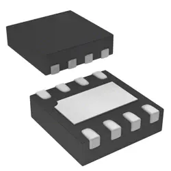
画像は参照用のみです。
XC7Z020-1CLG484I
IC SOC CORTEX-A9 667MHZ 484BGA
- メーカー
- Mfr。パート #XC7Z020-1CLG484I
- パッケージ CSBGA-484
- データシート
- 在庫中4498
100% オリジナル &新しい
出荷の準備ができている24時間
365日の保証
RFQおよびもっと割引を得る
仕様
| Package | Tray |
| Series | Zynq®-7000 |
| ProductStatus | Active |
| Architecture | MCU, FPGA |
| CoreProcessor | Dual ARM® Cortex®-A9 MPCore™ with CoreSight™ |
| RAMSize | 256KB |
| Peripherals | DMA |
| Connectivity | CANbus, EBI/EMI, Ethernet, I²C, MMC/SD/SDIO, SPI, UART/USART, USB OTG |
| Speed | 667MHz |
| PrimaryAttributes | Artix™-7 FPGA, 85K Logic Cells |
| OperatingTemperature | -40°C ~ 100°C (TJ) |
| Package/Case | 484-LFBGA, CSPBGA |
概要
Description
The XC7Z020-1CLG484I is a member of the Xilinx Zynq-7000 series, integrating a dual-core ARM Cortex-A9 processor with an FPGA fabric. It features 1 GB of DDR3 memory, up to 85,000 logic cells, and various I/O options, making it suitable for diverse applications such as embedded systems, industrial automation, automotive, and telecommunications.
This device operates at a maximum clock frequency of 1 GHz for the ARM cores and supports multiple interfaces, including Ethernet, USB, and PCIe. The combination of programmable logic and a powerful processing system allows for the development of complex applications that require both high-performance computing and real-time processing capabilities.
The XC7Z020-1CLG484I is packaged in a 484-ball FCG (Fine Pitch Ball Grid Array) format, which facilitates high-density designs. Its programmable nature enables flexibility in hardware configuration, making it ideal for rapid prototyping and development. Overall, the XC7Z020-1CLG484I is a versatile platform for engineers looking to leverage both software and hardware in their designs.
This device operates at a maximum clock frequency of 1 GHz for the ARM cores and supports multiple interfaces, including Ethernet, USB, and PCIe. The combination of programmable logic and a powerful processing system allows for the development of complex applications that require both high-performance computing and real-time processing capabilities.
The XC7Z020-1CLG484I is packaged in a 484-ball FCG (Fine Pitch Ball Grid Array) format, which facilitates high-density designs. Its programmable nature enables flexibility in hardware configuration, making it ideal for rapid prototyping and development. Overall, the XC7Z020-1CLG484I is a versatile platform for engineers looking to leverage both software and hardware in their designs.
Features
The XC7Z020-1CLG484I is a member of the Xilinx Zynq-7000 series, which combines a dual-core ARM Cortex-A9 processor with Xilinx 7-series FPGA fabric. Key features include:
1. Processing System: Dual-core ARM Cortex-A9 (up to 1 GHz), with memory management and various interfaces.
2. FPGA Fabric: 85,000 logic cells, 220 DSP slices, and 4,800 lookup tables (LUTs) for high-performance digital signal processing.
3. Memory Interfaces: Support for DDR3, DDR2, and LPDDR2 memory interfaces, with up to 1,066 MT/s data rates.
4. I/O Connectivity: 54 configurable I/O pins, supporting up to 16 SERDES for high-speed transceivers.
5. Integrated Peripherals: Includes USB, Ethernet, I²C, SPI, UART, and GPIO for versatile connectivity.
6. Low Power: Designed for efficient power consumption, making it suitable for embedded applications.
7. Development Tools: Compatible with Xilinx Vivado Design Suite for HDL and software application development.
This device is widely used in applications like automotive, industrial automation, and communications.
1. Processing System: Dual-core ARM Cortex-A9 (up to 1 GHz), with memory management and various interfaces.
2. FPGA Fabric: 85,000 logic cells, 220 DSP slices, and 4,800 lookup tables (LUTs) for high-performance digital signal processing.
3. Memory Interfaces: Support for DDR3, DDR2, and LPDDR2 memory interfaces, with up to 1,066 MT/s data rates.
4. I/O Connectivity: 54 configurable I/O pins, supporting up to 16 SERDES for high-speed transceivers.
5. Integrated Peripherals: Includes USB, Ethernet, I²C, SPI, UART, and GPIO for versatile connectivity.
6. Low Power: Designed for efficient power consumption, making it suitable for embedded applications.
7. Development Tools: Compatible with Xilinx Vivado Design Suite for HDL and software application development.
This device is widely used in applications like automotive, industrial automation, and communications.
Package
The XC7Z020-1CLG484I is packaged in a 484-ball FBGAs (Fine Pitch Ball Grid Array) package. This type of package is designed for high-density applications, offering efficient thermal performance and reliability in various electronic designs.
Pinout
The XC7Z020-1CLG484I is a part of the Xilinx Zynq-7000 series SoC, featuring a total of 484 pins. It integrates a dual-core ARM Cortex-A9 processor with programmable logic (FPGA).
Key functions of these pins include:
1. I/O Interfaces: Support for GPIO, I2C, SPI, UART, and other communication protocols.
2. Memory Interfaces: Connections for DDR3/DDR2 memory, including address, data, and control signals.
3. Configuration and JTAG: Pins for device programming and debugging.
4. Power and Ground: Dedicated pins for power supply and ground connections.
5. Clock Inputs: Pins for inputting clock signals for system timing.
The XC7Z020-1CLG484I is commonly used in applications requiring embedded processing combined with high-performance FPGA capabilities.
Key functions of these pins include:
1. I/O Interfaces: Support for GPIO, I2C, SPI, UART, and other communication protocols.
2. Memory Interfaces: Connections for DDR3/DDR2 memory, including address, data, and control signals.
3. Configuration and JTAG: Pins for device programming and debugging.
4. Power and Ground: Dedicated pins for power supply and ground connections.
5. Clock Inputs: Pins for inputting clock signals for system timing.
The XC7Z020-1CLG484I is commonly used in applications requiring embedded processing combined with high-performance FPGA capabilities.
Manufacturer
The XC7Z020-1CLG484I is manufactured by Xilinx, Inc., a company that specializes in programmable logic devices and solutions. Founded in 1984 and headquartered in San Jose, California, Xilinx is known for its field-programmable gate arrays (FPGAs), complex programmable logic devices (CPLDs), and system-on-chip (SoC) solutions. The XC7Z020-1CLG484I is part of the Zynq-7000 series, which integrates a dual-core ARM Cortex-A9 processor with FPGA fabric, making it suitable for various applications including embedded systems, digital signal processing, and high-performance computing. In 2020, Xilinx was acquired by AMD, further expanding its portfolio in the semiconductor industry.
Application
The XC7Z020-1CLG484I, part of the Zynq-7000 series, is used in various application areas, including embedded systems, industrial automation, automotive systems, medical devices, robotics, and telecommunications. Its strengths in processing, programmable logic, and connectivity make it suitable for high-performance tasks such as image processing, signal processing, and real-time data analysis, enabling intelligent applications across multiple industries.
Equivalent
The XC7Z020-1CLG484I chip is part of the Xilinx Zynq-7000 series. Equivalent products include:
1. XC7Z010-1CLG400I - A lower density variant.
2. XC7Z030-1CLG484I - A higher density option.
3. XC7Z020-1CLG484C - A commercial grade version.
4. XC7Z020-1FBG484I - A different package variant.
Always verify compatibility based on specific application requirements.
1. XC7Z010-1CLG400I - A lower density variant.
2. XC7Z030-1CLG484I - A higher density option.
3. XC7Z020-1CLG484C - A commercial grade version.
4. XC7Z020-1FBG484I - A different package variant.
Always verify compatibility based on specific application requirements.
出荷
出荷方法私たち
DHL、FedEx、TNT、UPS、またはあなたの選択の他の運送業者を通じてグローバルな出荷サービスを提供します。
出荷料参照(DHL/FedEx):
DHL の: 配送費は25ドル〜45ドル(0.5kg)の範囲で、推定配送時間は2〜5営業日です。
フェデックス: 配送費は25ドル〜40ドル(0.5kg)の範囲で、推定配送時間は3〜7営業日。
UPS の: 配送費は25ドル〜45ドル(0.5kg)の範囲で、推定配送時間は3〜7営業日。
TNT社: 配送費は25ドル〜65ドル(0.5kg)の範囲で、推定配送時間は3〜7営業日。
EMS: 配送料金は30〜50ドル(0.5kg)の範囲で、推定配送時間は7〜15営業日です。
登録航空郵便: 配送費は2〜4ドル(0.1kg)で、推定配送時間は5〜20営業日です。
支払い
Payment Methods
支払い期間は100%前払いです。
現在、下記の支払い方法のみを受け入れています。:
1. ペイパル
2. クレジット・デビットカード
3. ワイヤー 転送
類似
-
![MX25R8035FM1IL0]() MX25R8035FM1IL0
Macronix
-
![MX25V1635FZNI]() MX25V1635FZNI
Macronix
-
![MX29F400CBTI-70G]() MX29F400CBTI-70G
Macronix
-
![MX66U1G45GXDI00]() MX66U1G45GXDI00
Macronix
-
![MX25V2033FM1I]() MX25V2033FM1I
Macronix
-
![MX25R3235FZNIL0]() MX25R3235FZNIL0
Macronix
-
![MX30LF2G28AD-TI]() MX30LF2G28AD-TI
Macronix
-
![MX25L25673GMI-08G]() MX25L25673GMI-08G
Macronix
-
![MX29GL512FHXFI-11G]() MX29GL512FHXFI-11..
Macronix
-
![MX25R1635FZUIH0]() MX25R1635FZUIH0
Macronix
-
![MX25L6433FM2I-08G]() MX25L6433FM2I-08G
Macronix
-
![MX25U25645GXDI00]() MX25U25645GXDI00
Macronix