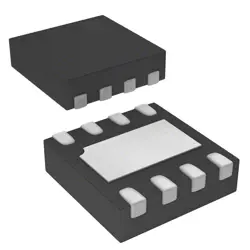
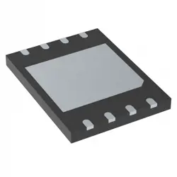
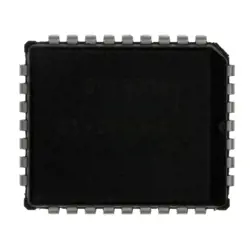
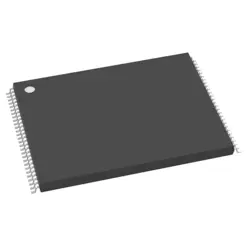
画像は参照用のみです。
XC6SLX9-2CSG324I
IC FPGA 200 I/O 324CSBGA
- メーカー
- Mfr。パート #XC6SLX9-2CSG324I
- パッケージ BGA-324
- データシート
- 在庫中6045
100% オリジナル &新しい
出荷の準備ができている24時間
365日の保証
RFQおよびもっと割引を得る
仕様
| Package | Tray |
| Series | Spartan®-6 LX |
| ProductStatus | Active |
| NumberofLABs/CLBs | 715 |
| NumberofLogicElements/Cells | 9152 |
| TotalRAMBits | 589824 |
| NumberofI/O | 200 |
| Voltage-Supply | 1.14V ~ 1.26V |
| MountingType | Surface Mount |
| OperatingTemperature | -40°C ~ 100°C (TJ) |
| Package/Case | 324-LFBGA, CSPBGA |
概要
Description
The XC6SLX9-2CSG324I is a member of the Xilinx Spartan-6 family of FPGAs (Field Programmable Gate Arrays). It features 9,152 logic cells and supports a range of applications from consumer electronics to industrial automation. The device is built on a 45nm process technology and operates with a maximum clock frequency of up to 550 MHz.
It comes in a CSG324 package, which features 324 pins for flexible connectivity and integration in various designs. The XC6SLX9 includes several key resources such as DSP slices, block RAM, and a rich set of I/O standards, making it suitable for tasks requiring high-speed data processing and efficient resource management.
The "-2" indicates the speed grade, denoting a relatively faster performance within the Spartan-6 family. The device supports a variety of development tools and is compatible with Xilinx's ISE design suite, enabling users to implement complex digital designs efficiently. Overall, the XC6SLX9-2CSG324I is a versatile and cost-effective solution for a broad range of applications.
It comes in a CSG324 package, which features 324 pins for flexible connectivity and integration in various designs. The XC6SLX9 includes several key resources such as DSP slices, block RAM, and a rich set of I/O standards, making it suitable for tasks requiring high-speed data processing and efficient resource management.
The "-2" indicates the speed grade, denoting a relatively faster performance within the Spartan-6 family. The device supports a variety of development tools and is compatible with Xilinx's ISE design suite, enabling users to implement complex digital designs efficiently. Overall, the XC6SLX9-2CSG324I is a versatile and cost-effective solution for a broad range of applications.
Features
The XC6SLX9-2CSG324I is a member of the Xilinx Spartan-6 FPGA family, designed for cost-sensitive applications. Key features include:
1. Logic Cells: It offers 9,152 logic cells, enabling complex designs.
2. Registers: Each logic cell includes a configurable register for versatile operations.
3. DSP Slices: Contains 18 DSP slices optimized for digital signal processing tasks.
4. Block RAM: Features 576 Kbits of block RAM for data storage.
5. I/O Pins: Up to 24 differential I/O pairs and multiple LVDS channels for high-speed communication.
6. Speed Grade: Rated at -2, providing a maximum performance of 200 MHz.
7. Power Efficiency: Designed for low power consumption, making it suitable for battery-operated devices.
8. Configuration: Supports multiple configuration modes, including JTAG and SPI.
9. Temperature Range: Ideal for industrial applications with extended temperature ratings.
These attributes make the XC6SLX9-2CSG324I suitable for a variety of applications, including automotive, communications, and consumer electronics.
1. Logic Cells: It offers 9,152 logic cells, enabling complex designs.
2. Registers: Each logic cell includes a configurable register for versatile operations.
3. DSP Slices: Contains 18 DSP slices optimized for digital signal processing tasks.
4. Block RAM: Features 576 Kbits of block RAM for data storage.
5. I/O Pins: Up to 24 differential I/O pairs and multiple LVDS channels for high-speed communication.
6. Speed Grade: Rated at -2, providing a maximum performance of 200 MHz.
7. Power Efficiency: Designed for low power consumption, making it suitable for battery-operated devices.
8. Configuration: Supports multiple configuration modes, including JTAG and SPI.
9. Temperature Range: Ideal for industrial applications with extended temperature ratings.
These attributes make the XC6SLX9-2CSG324I suitable for a variety of applications, including automotive, communications, and consumer electronics.
Package
The XC6SLX9-2CSG324I is packaged in a CSG324 form factor, which is a Fine-Pitch Ball Grid Array (FBGA) package. It has 324 balls for connectivity and is designed for high-density applications, providing efficient thermal performance and smaller footprint.
Pinout
The XC6SLX9-2CSG324I is a member of the Xilinx Spartan-6 FPGA family. It features a total of 324 pins.
The primary functions of these pins can be categorized as follows:
1. I/O Pins: Configurable for general-purpose input/output, supporting various voltage levels and signaling standards.
2. Power Pins: Dedicated pins for power supply (VCCINT, VCCIO) and ground (GND).
3. Configuration Pins: Pins used for the configuration process, such as the JTAG interface and configuration modes.
4. Clock Pins: Specific pins for clock inputs, which are essential for timing management within the FPGA.
This device is designed for a range of applications, including digital signal processing, communications, and embedded control systems, offering a balance of performance and flexibility in design.
The primary functions of these pins can be categorized as follows:
1. I/O Pins: Configurable for general-purpose input/output, supporting various voltage levels and signaling standards.
2. Power Pins: Dedicated pins for power supply (VCCINT, VCCIO) and ground (GND).
3. Configuration Pins: Pins used for the configuration process, such as the JTAG interface and configuration modes.
4. Clock Pins: Specific pins for clock inputs, which are essential for timing management within the FPGA.
This device is designed for a range of applications, including digital signal processing, communications, and embedded control systems, offering a balance of performance and flexibility in design.
Manufacturer
The manufacturer of the XC6SLX9-2CSG324I is Xilinx, Inc. Xilinx is a leading technology company that specializes in the development and production of programmable logic devices, including Field-Programmable Gate Arrays (FPGAs), complex programmable logic devices (CPLDs), and associated software tools for design and development. Founded in 1984, Xilinx is known for pioneering the FPGA technology and providing solutions for various industries, including telecommunications, automotive, aerospace, defense, and consumer electronics. The XC6SLX9-2CSG324I is part of the Spartan-6 FPGA family, which is designed for cost-sensitive applications requiring low power and high performance. In 2020, Xilinx was acquired by AMD, further expanding its capabilities in the semiconductor industry.
Application
The XC6SLX9-2CSG324I is a Low-Power Spartan-6 FPGA commonly used in applications such as industrial automation, telecommunications, automotive systems, medical devices, and consumer electronics. It is suitable for tasks like digital signal processing, real-time data acquisition, and control systems due to its flexibility, performance, and low power consumption.
Equivalent
The XC6SLX9-2CSG324I is a Spartan-6 FPGA from Xilinx. Equivalent products include the Lattice ECP5 (e.g., LFE5U-85F) and the Intel/Altera Cyclone IV (e.g., EP4CE9). For more specific needs, consider other Spartan-6 variants or newer families like Xilinx's Artix-7, which may offer similar or improved capabilities. Always verify specific features and pin compatibility before substitution.
出荷
出荷方法私たち
DHL、FedEx、TNT、UPS、またはあなたの選択の他の運送業者を通じてグローバルな出荷サービスを提供します。
出荷料参照(DHL/FedEx):
DHL の: 配送費は25ドル〜45ドル(0.5kg)の範囲で、推定配送時間は2〜5営業日です。
フェデックス: 配送費は25ドル〜40ドル(0.5kg)の範囲で、推定配送時間は3〜7営業日。
UPS の: 配送費は25ドル〜45ドル(0.5kg)の範囲で、推定配送時間は3〜7営業日。
TNT社: 配送費は25ドル〜65ドル(0.5kg)の範囲で、推定配送時間は3〜7営業日。
EMS: 配送料金は30〜50ドル(0.5kg)の範囲で、推定配送時間は7〜15営業日です。
登録航空郵便: 配送費は2〜4ドル(0.1kg)で、推定配送時間は5〜20営業日です。
支払い
Payment Methods
支払い期間は100%前払いです。
現在、下記の支払い方法のみを受け入れています。:
1. ペイパル
2. クレジット・デビットカード
3. ワイヤー 転送
類似
-
![MX25L3233FM1I-08Q]() MX25L3233FM1I-08Q
Macronix
-
![MX25V4035FZUI]() MX25V4035FZUI
Macronix
-
![MX25V2033FM1I]() MX25V2033FM1I
Macronix
-
![MX25L8035EM2I-10G]() MX25L8035EM2I-10G
Macronix
-
![MX25L25673GMI-08G]() MX25L25673GMI-08G
Macronix
-
![MX25U51279GXDR00]() MX25U51279GXDR00
Macronix
-
![MX25L2006EM1I-12G]() MX25L2006EM1I-12G
Macronix
-
![MX25U3232FZBI02]() MX25U3232FZBI02
Macronix
-
![MX25L12833FZ2I-10G]() MX25L12833FZ2I-10..
Macronix
-
![MX29F040CQI-70G]() MX29F040CQI-70G
Macronix
-
![MX29F800CBTI-70G]() MX29F800CBTI-70G
Macronix
-
![MX29LV640ETTI-70G]() MX29LV640ETTI-70G
Macronix