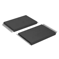
画像は参照用のみです。
XC17S50APD8I
IC PROM SER 50000 I-TEMP 8-DIP
- メーカー
- Mfr。パート #XC17S50APD8I
- パッケージ
- データシート
- 在庫中7194
100% オリジナル &新しい
出荷の準備ができている24時間
365日の保証
RFQおよびもっと割引を得る
仕様
| Part Status | Obsolete |
| Base Product Number | XC17S50A |
| DigiKey Programmable | Not Verified |
| Programmable Type | OTP |
| Memory Size | 500kb |
| Voltage - Supply | 3V ~ 3.6V |
| Operating Temperature | -40°C ~ 85°C |
| Mounting Type | Through Hole |
| Package | 8-DIP (0.300", 7.62mm) |
| Supplier Device Package | 8-PDIP |
| Packaging | Tube |
概要
Description
The XC17S50APD8I is a part of the Xilinx XC17 series of programmable logic devices, specifically designed for configuration and enhancement of FPGA applications. It features a 5V, 50,000-bit serial configuration memory that allows for the storage of FPGA configuration data. The device operates on a 16-pin DIP or a 20-pin surface mount package, making it versatile for various designs.
Key characteristics include a fast programming speed, low power consumption, and robust data retention, making it suitable for applications like system configuration, firmware upgrades, and embedded systems. The XC17S50APD8I supports multiple programming options, including JTAG, and is compatible with various Xilinx FPGA families.
In summary, the XC17S50APD8I is an essential component for users looking to implement efficient and flexible configuration solutions in their FPGA designs.
Features
The XC17S50APD8I is a programmable logic device (PLD) from Xilinx's XC17 series, primarily designed for applications requiring in-system programmability. Key features include:
1. Capacity: It offers 50 macrocells, allowing for the implementation of complex logic functions.
2. Speed: The device operates with a maximum propagation delay of approximately 10 ns, suitable for high-speed applications.
3. Voltage: It supports a 3.3V power supply, making it compatible with modern low-voltage systems.
4. In-System Programmability: The XC17S50APD8I can be programmed and reprogrammed in-circuit, enabling design flexibility and quick iterations.
5. Configuration: Supports various configuration methods, including JTAG and serial programming.
6. Temperature Range: Typically rated for industrial temperature ranges, enhancing reliability in diverse environments.
7. Package Type: Available in a 64-pin TQFP package, facilitating integration into compact designs.
These features make the XC17S50APD8I suitable for applications in telecommunications, automotive, and consumer electronics where adaptability and performance are critical.
Package
The XC17S50APD8I is packaged in a 20-pin Dual In-line Package (DIP). This type of package facilitates easy mounting on printed circuit boards (PCBs) and is suitable for various applications requiring programmable logic devices.
Pinout
The XC17S50APD8I is a 16-pin Integrated Circuit (IC) from Xilinx, part of the XC17 series of Programmable Logic Devices. This specific device is a configuration PROM (Programmable Read-Only Memory) designed for programming Xilinx FPGAs.
### Pin Count:
- Total Pins: 16
### Pin Functions:
1. VCC: Power supply input.
2. GND: Ground connection.
3. CS (Chip Select): Activates the device for communication.
4. SK (Serial Clock): Controls the timing of data transfer.
5. SI (Serial Input): Receives data for programming.
6. SO (Serial Output): Sends data out, typically for reading.
7. WP (Write Protect): Protects the contents from being accidentally altered.
8. BUSY: Indicates the current operation status (busy or ready).
9. TDO (Test Data Out): Used in JTAG programming.
10. TDI (Test Data In): Receives data in JTAG mode.
11. TCK (Test Clock): Provides clock input for JTAG operations.
12. TMS (Test Mode Select): Controls the state machine for JTAG.
This device is primarily used for storing configuration data for FPGAs.
Manufacturer
The XC17S50APD8I is manufactured by Xilinx, Inc., which is a leading company in the field of programmable logic devices and FPGAs (Field Programmable Gate Arrays). Xilinx specializes in providing advanced semiconductor solutions for various applications, including telecommunications, automotive, data centers, and industrial automation. The XC17S50APD8I is specifically a configuration memory device used for programming Xilinx FPGAs. Xilinx was founded in 1984 and has been at the forefront of innovation in the programmable logic market, contributing significantly to the evolution of digital design and hardware acceleration. In 2020, Xilinx was acquired by AMD (Advanced Micro Devices), further expanding its impact in high-performance computing and adaptive computing technologies.
Application
The XC17S50APD8I is a configuration memory device used primarily in FPGA and CPLD applications. Its key areas include embedded systems, telecommunications, automotive electronics, industrial automation, and consumer electronics. It serves to store configuration data for programmable logic devices, enabling rapid reconfiguration and enhancing system flexibility.
Equivalent
The XC17S50APD8I is a CPLD (Complex Programmable Logic Device) from Xilinx. Equivalent products include:
1. ATF1502AS by Atmel
2. Lattice ispLSI 1016 by Lattice Semiconductor
3. MAX 7000S by Altera (now Intel)
These devices offer similar functionality and usage but check specific features and pin configurations for compatibility.
1. ATF1502AS by Atmel
2. Lattice ispLSI 1016 by Lattice Semiconductor
3. MAX 7000S by Altera (now Intel)
These devices offer similar functionality and usage but check specific features and pin configurations for compatibility.
出荷
出荷方法私たち
DHL、FedEx、TNT、UPS、またはあなたの選択の他の運送業者を通じてグローバルな出荷サービスを提供します。
出荷料参照(DHL/FedEx):
DHL の: 配送費は25ドル〜45ドル(0.5kg)の範囲で、推定配送時間は2〜5営業日です。
フェデックス: 配送費は25ドル〜40ドル(0.5kg)の範囲で、推定配送時間は3〜7営業日。
UPS の: 配送費は25ドル〜45ドル(0.5kg)の範囲で、推定配送時間は3〜7営業日。
TNT社: 配送費は25ドル〜65ドル(0.5kg)の範囲で、推定配送時間は3〜7営業日。
EMS: 配送料金は30〜50ドル(0.5kg)の範囲で、推定配送時間は7〜15営業日です。
登録航空郵便: 配送費は2〜4ドル(0.1kg)で、推定配送時間は5〜20営業日です。
支払い
Payment Methods
支払い期間は100%前払いです。
現在、下記の支払い方法のみを受け入れています。:
1. ペイパル
2. クレジット・デビットカード
3. ワイヤー 転送
類似
-
![MX25L3233FZBI-08Q]() MX25L3233FZBI-08Q
Macronix
-
![MX29F400CBTI-70G]() MX29F400CBTI-70G
Macronix
-
![MX25V2033FM1I]() MX25V2033FM1I
Macronix
-
![MX25V16066M1I02]() MX25V16066M1I02
Macronix
-
![MX25R1635FZUIH0]() MX25R1635FZUIH0
Macronix
-
![MX25V1635FM2I]() MX25V1635FM2I
Macronix
-
![MX25L12833FM2I-10G]() MX25L12833FM2I-10..
Macronix
-
![MX25L12833FZNI-10G]() MX25L12833FZNI-10..
Macronix
-
![MX29F040CQI-70G]() MX29F040CQI-70G
Macronix
-
![MX29F040CTI-70G]() MX29F040CTI-70G
Macronix
-
![MX29F800CBTI-70G]() MX29F800CBTI-70G
Macronix
-
![MX25U51245GZ4I00]() MX25U51245GZ4I00
Macronix