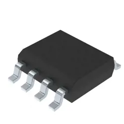
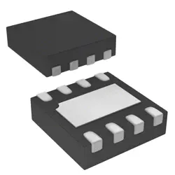
画像は参照用のみです。
W9825G6KH-6I
IC DRAM 256MBIT PAR 54TSOP II
- メーカー
- Mfr。パート #W9825G6KH-6I
- パッケージ
- データシート W9825G6KH-6I DataSheet
- 在庫中2373
100% オリジナル &新しい
出荷の準備ができている24時間
365日の保証
RFQおよびもっと割引を得る
仕様
| Part Status | Active |
| Base Product Number | W9825G6 |
| DigiKey Programmable | Not Verified |
| Memory Type | Volatile |
| Memory Format | DRAM |
| Technology | SDRAM |
| Memory Size | 256Mbit |
| Memory Organization | 16M x 16 |
| Memory Interface | Parallel |
| Clock Frequency | 166 MHz |
| Voltage - Supply | 3V ~ 3.6V |
| Operating Temperature | -40°C ~ 85°C (TA) |
| Mounting Type | Surface Mount |
| Package | 54-TSOP (0.400", 10.16mm Width) |
| Supplier Device Package | 54-TSOP II |
| Packaging | Tray |
| Access Time | 5 ns |
概要
Description
The W9825G6KH-6I is a DRAM (Dynamic Random Access Memory) chip produced by Winbond. It is a 256Mbit (32MB) DDR2 SDRAM device, designed for use in various computing applications, including servers, desktops, and laptops. The "6I" designation indicates a specific speed and performance rating; in this case, it typically operates at a clock speed of 400 MHz with a data rate of 800 MT/s (megatransfers per second).
This memory chip features a 16-bit data bus and uses a 1.8V power supply, making it energy-efficient compared to earlier memory technologies. It supports various memory functions, including burst modes and multiple bank operations, which enhance data processing speeds. The W9825G6KH-6I is known for its reliability and is suitable for applications requiring high performance and stability.
This memory chip features a 16-bit data bus and uses a 1.8V power supply, making it energy-efficient compared to earlier memory technologies. It supports various memory functions, including burst modes and multiple bank operations, which enhance data processing speeds. The W9825G6KH-6I is known for its reliability and is suitable for applications requiring high performance and stability.
Features
The W9825G6KH-6I is a DRAM memory chip from Winbond, specifically designed for high-performance applications. It features a 512Mb capacity and operates on a 1.8V power supply. This device is built using a 90nm manufacturing process and offers fast access times, typically around 6ns. It supports a number of advanced functionalities such as deep power-down modes, easy data retention, and extended refresh cycles, which enhance energy efficiency and performance stability.
Additionally, the W9825G6KH-6I is compatible with the DDR2 SDRAM standards, allowing for high-speed data transfers and improved bandwidth. Its package options include standard TSOPII, making it suitable for various electronic devices, including smartphones, tablets, and other consumer electronics. Overall, it is designed for applications requiring reliable, high-speed memory solutions.
Additionally, the W9825G6KH-6I is compatible with the DDR2 SDRAM standards, allowing for high-speed data transfers and improved bandwidth. Its package options include standard TSOPII, making it suitable for various electronic devices, including smartphones, tablets, and other consumer electronics. Overall, it is designed for applications requiring reliable, high-speed memory solutions.
Package
The W9825G6KH-6I is a DRAM memory chip packaged in a standard 54-ball FBGA (Fine Ball Grid Array) format. This package type is designed for high-density applications and provides efficient thermal management and space-saving benefits for electronic devices.
Pinout
The W9825G6KH-6I is a DRAM (Dynamic Random Access Memory) component from Winbond, specifically a DDR3 SDRAM. It typically comes in a 78-ball TFBGA (thin fine-pitch ball grid array) package. The pin count for this device is 78.
The primary functions of the pins include:
1. Data Inputs/Outputs (DQ): These pins are used for data transfer, allowing input and output of data bits during read and write operations.
2. Address Inputs (A): These pins are used to select memory addresses for read/write operations.
3. Control Pins (CS, RAS, CAS, WE): These control signals manage the operation of the memory, such as chip selection and read/write commands.
4. Clock Input (CLK): The clock signal synchronizes data transfers.
5. Power and Ground Pins (VDD, VSS): These provide the necessary power supply and ground connections for the device's operation.
The W9825G6KH-6I operates at a voltage of 1.5V and has a speed grade of 6, indicating its performance capabilities.
Manufacturer
The W9825G6KH-6I is manufactured by Winbond Electronics Corporation, a Taiwanese semiconductor company. Winbond specializes in the design and production of memory solutions, particularly DRAM (Dynamic Random-Access Memory) and Flash memory products. Founded in 1987, the company focuses on providing high-quality memory products for various applications, including consumer electronics, automotive, and industrial sectors. Winbond is known for its innovation in memory technology and has established a significant presence in the global semiconductor market.
Application
The W9825G6KH-6I is a DDR2 SDRAM memory chip primarily used in consumer electronics, such as laptops, desktops, and gaming consoles. It is suitable for applications requiring high-speed data processing and storage, including graphics rendering, multimedia playback, and general computing tasks. Additionally, it can be used in networking equipment and embedded systems that demand reliable memory performance.
Equivalent
The W9825G6KH-6I chip is a 512Mb DDR2 SDRAM memory chip. Equivalent products include the Micron MT46V64M8, Samsung K4T1G164QE, and Hynix HY5PS1G831C. These alternatives generally share similar specifications, such as organization, voltage, and timing parameters. Always check datasheets for precise compatibility.
出荷
出荷方法私たち
DHL、FedEx、TNT、UPS、またはあなたの選択の他の運送業者を通じてグローバルな出荷サービスを提供します。
出荷料参照(DHL/FedEx):
DHL の: 配送費は25ドル〜45ドル(0.5kg)の範囲で、推定配送時間は2〜5営業日です。
フェデックス: 配送費は25ドル〜40ドル(0.5kg)の範囲で、推定配送時間は3〜7営業日。
UPS の: 配送費は25ドル〜45ドル(0.5kg)の範囲で、推定配送時間は3〜7営業日。
TNT社: 配送費は25ドル〜65ドル(0.5kg)の範囲で、推定配送時間は3〜7営業日。
EMS: 配送料金は30〜50ドル(0.5kg)の範囲で、推定配送時間は7〜15営業日です。
登録航空郵便: 配送費は2〜4ドル(0.1kg)で、推定配送時間は5〜20営業日です。
支払い
Payment Methods
支払い期間は100%前払いです。
現在、下記の支払い方法のみを受け入れています。:
1. ペイパル
2. クレジット・デビットカード
3. ワイヤー 転送
類似
-
![MX25L3233FM1I-08Q]() MX25L3233FM1I-08Q
Macronix
-
![MX29F400CBTI-70G]() MX29F400CBTI-70G
Macronix
-
![MX25V2033FM1I]() MX25V2033FM1I
Macronix
-
![MX25V16066M2I02]() MX25V16066M2I02
Macronix
-
![MX30LF2G28AD-TI]() MX30LF2G28AD-TI
Macronix
-
![MX25L25673GMI-10G]() MX25L25673GMI-10G
Macronix
-
![MX29GL512FHXFI-11G]() MX29GL512FHXFI-11..
Macronix
-
![MX25V1635FM2I]() MX25V1635FM2I
Macronix
-
![MX25U3232FZBI02]() MX25U3232FZBI02
Macronix
-
![MX25L12833FZ2I-10G]() MX25L12833FZ2I-10..
Macronix
-
![MX25L12835FZ2I-10G]() MX25L12835FZ2I-10..
Macronix
-
![MX25U51245GZ4I00]() MX25U51245GZ4I00
Macronix