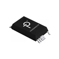
画像は参照用のみです。
UCC27282QDRQ1
IC GATE DRVR HALF-BRIDGE 8SOIC
- メーカー
- Mfr。パート #UCC27282QDRQ1
- パッケージ
- データシート UCC27282QDRQ1 DataSheet
- 在庫中2949
100% オリジナル &新しい
出荷の準備ができている24時間
365日の保証
RFQおよびもっと割引を得る
仕様
| Part Status | Active |
| DigiKey Programmable | Not Verified |
| Driven Configuration | Half-Bridge |
| Channel Type | Independent |
| Number of Drivers | 2 |
| Gate Type | MOSFET (N-Channel) |
| Voltage - Supply | 5.5V ~ 16V |
| Logic Voltage - VIL, VIH | 0.9V, 2.4V |
| Current - Peak Output (Source, Sink) | 2.5A, 3.5A |
| Input Type | Non-Inverting |
| Rise / Fall Time (Typ) | 12ns, 10ns |
| Operating Temperature | -40°C ~ 125°C |
| Mounting Type | Surface Mount |
| Package / Case | 8-SOIC (0.154", 3.90mm Width) |
| Supplier Device Package | 8-SOIC |
| Base Product Number | UCC27282 |
| High Side Voltage - Max (Bootstrap) | 120 V |
| Grade | Automotive |
| Qualification | AEC-Q100 |
概要
Description
The UCC27282QDRQ1 is a high-frequency, high-side and low-side gate driver developed by Texas Instruments. It is designed to drive power MOSFETs and IGBTs in various switching power applications, such as synchronous buck converters, half-bridge, full-bridge, and three-phase configurations. The driver features a 120-V maximum bootstrap supply voltage with robust protection mechanisms, ensuring reliable operation in harsh environments. It offers a 4-A peak sourcing and 5-A peak sinking current capability, providing efficient switching performance.
Key features include a 20-ns propagation delay, undervoltage lockout (UVLO) for both high-side and low-side drivers, and a wide input voltage range. Additionally, it supports a maximum switching frequency up to 1 MHz, making it suitable for high-speed applications. The UCC27282QDRQ1 is housed in a thermally enhanced, space-efficient SOIC package, favoring compact design requirements.
This driver is AEC-Q100 qualified, confirming its suitability for automotive and other demanding applications. Its robust design, combined with efficient power handling capabilities, make it an optimal choice for engineers looking to enhance the performance and reliability of their power management systems.
Key features include a 20-ns propagation delay, undervoltage lockout (UVLO) for both high-side and low-side drivers, and a wide input voltage range. Additionally, it supports a maximum switching frequency up to 1 MHz, making it suitable for high-speed applications. The UCC27282QDRQ1 is housed in a thermally enhanced, space-efficient SOIC package, favoring compact design requirements.
This driver is AEC-Q100 qualified, confirming its suitability for automotive and other demanding applications. Its robust design, combined with efficient power handling capabilities, make it an optimal choice for engineers looking to enhance the performance and reliability of their power management systems.
Features
The UCC27282QDRQ1 is a high-frequency, high-side/low-side gate driver designed for driving power MOSFETs and IGBTs. Key features include:
1. High-Speed Operation: It provides fast switching speeds suitable for applications requiring rapid operation.
2. Wide Operating Voltage Range: The device can handle a wide range of input voltages, making it versatile for various applications.
3. Low Propagation Delay: This feature helps reduce the switching losses by ensuring quick transitions in power devices.
4. High Output Current Capability: It offers strong drive strength to enable the efficient operation of large power MOSFETs or IGBTs.
5. UVLO Protection: Under Voltage Lockout (UVLO) ensures the device operates only when the supply voltage is above a certain threshold, protecting the driver and the MOSFETs/IGBTs.
6. Thermal Protection: Built-in thermal protection ensures reliability by preventing overheating under high-load conditions.
7. Automotive Qualification: As a Q1 component, it meets automotive reliability standards, making it suitable for automotive applications.
These features make the UCC27282QDRQ1 a robust choice for high-performance switching applications, especially in automotive environments.
1. High-Speed Operation: It provides fast switching speeds suitable for applications requiring rapid operation.
2. Wide Operating Voltage Range: The device can handle a wide range of input voltages, making it versatile for various applications.
3. Low Propagation Delay: This feature helps reduce the switching losses by ensuring quick transitions in power devices.
4. High Output Current Capability: It offers strong drive strength to enable the efficient operation of large power MOSFETs or IGBTs.
5. UVLO Protection: Under Voltage Lockout (UVLO) ensures the device operates only when the supply voltage is above a certain threshold, protecting the driver and the MOSFETs/IGBTs.
6. Thermal Protection: Built-in thermal protection ensures reliability by preventing overheating under high-load conditions.
7. Automotive Qualification: As a Q1 component, it meets automotive reliability standards, making it suitable for automotive applications.
These features make the UCC27282QDRQ1 a robust choice for high-performance switching applications, especially in automotive environments.
Package
The UCC27282QDRQ1 is a gate driver IC that comes in an 8-pin SOIC (Small Outline Integrated Circuit) package. This package type is compact and commonly used for surface-mount applications, providing reliable performance for driving high-side and low-side power MOSFETs.
Pinout
The UCC27282QDRQ1 is a gate driver IC from Texas Instruments designed for driving power MOSFETs and IGBTs. It typically comes in an 8-pin package. Here’s a brief overview of its pin functions:
1. VDD: Supply Voltage pin for the driver.
2. HB: High-Side Bootstrap Voltage input.
3. HS: High-Side MOSFET Source connection.
4. HO: High-Side Gate Drive Output.
5. VSS: Ground connection for the IC.
6. LO: Low-Side Gate Drive Output.
7. LIN: Low-Side Input. Controls the low-side driver.
8. HIN: High-Side Input. Controls the high-side driver.
The UCC27282QDRQ1 is characterized by features such as high-speed operation, high drive current capability, and robustness suitable for automotive applications. It is used to efficiently switch high-power devices in a variety of power supply and motor control applications.
1. VDD: Supply Voltage pin for the driver.
2. HB: High-Side Bootstrap Voltage input.
3. HS: High-Side MOSFET Source connection.
4. HO: High-Side Gate Drive Output.
5. VSS: Ground connection for the IC.
6. LO: Low-Side Gate Drive Output.
7. LIN: Low-Side Input. Controls the low-side driver.
8. HIN: High-Side Input. Controls the high-side driver.
The UCC27282QDRQ1 is characterized by features such as high-speed operation, high drive current capability, and robustness suitable for automotive applications. It is used to efficiently switch high-power devices in a variety of power supply and motor control applications.
Manufacturer
The UCC27282QDRQ1 is manufactured by Texas Instruments. Texas Instruments (TI) is a global technology company known for designing and manufacturing semiconductors and integrated circuits, which are used in a wide array of electronic devices. TI focuses on developing solutions for analog and embedded processing, serving diverse markets such as automotive, industrial, personal electronics, and communications equipment.
Application
The UCC27282QDRQ1 is a high-side/low-side gate driver designed for automotive applications. It is commonly used in areas such as DC-DC converters, synchronous rectification, motor drives, and power supplies in automotive systems. Its robust design is suited for driving power MOSFETs and IGBTs, making it ideal for electric vehicle powertrains, fuel pump controls, and other high-efficiency power management applications in the automotive industry.
Equivalent
The UCC27282QDRQ1 is a high-speed gate driver from Texas Instruments. Equivalent products include the Infineon 2ED2183S06F, ON Semiconductor NCP51820, and Analog Devices ADuM3223. These alternatives offer similar functionalities such as high-side/low-side gate driving, fast switching speeds, and are suitable for driving power MOSFETs and IGBTs in various applications. Always check the specific datasheets for compatibility with your application requirements.
出荷
出荷方法私たち
DHL、FedEx、TNT、UPS、またはあなたの選択の他の運送業者を通じてグローバルな出荷サービスを提供します。
出荷料参照(DHL/FedEx):
DHL の: 配送費は25ドル〜45ドル(0.5kg)の範囲で、推定配送時間は2〜5営業日です。
フェデックス: 配送費は25ドル〜40ドル(0.5kg)の範囲で、推定配送時間は3〜7営業日。
UPS の: 配送費は25ドル〜45ドル(0.5kg)の範囲で、推定配送時間は3〜7営業日。
TNT社: 配送費は25ドル〜65ドル(0.5kg)の範囲で、推定配送時間は3〜7営業日。
EMS: 配送料金は30〜50ドル(0.5kg)の範囲で、推定配送時間は7〜15営業日です。
登録航空郵便: 配送費は2〜4ドル(0.1kg)で、推定配送時間は5〜20営業日です。
支払い
Payment Methods
支払い期間は100%前払いです。
現在、下記の支払い方法のみを受け入れています。:
1. ペイパル
2. クレジット・デビットカード
3. ワイヤー 転送
類似
-
![MX25R8035FM1IL0]() MX25R8035FM1IL0
MX25R8035FM1IL0
Macronix
-
![MX66U1G45GXDI00]() MX66U1G45GXDI00
MX66U1G45GXDI00
Macronix
-
![MX25R3235FZNIL0]() MX25R3235FZNIL0
MX25R3235FZNIL0
Macronix
-
![MX25R6435FBDIL0]() MX25R6435FBDIL0
MX25R6435FBDIL0
Macronix
-
![MX29GL512FHXFI-11G]() MX29GL512FHXFI-11..
MX29GL512FHXFI-11..
Macronix
-
![MX25L12833FM2I-10G]() MX25L12833FM2I-10..
MX25L12833FM2I-10..
Macronix
-
![MX29F040CQI-70G]() MX29F040CQI-70G
MX29F040CQI-70G
Macronix
-
![MX29F040CTI-70G]() MX29F040CTI-70G
MX29F040CTI-70G
Macronix
-
![MX29LV640ETTI-70G]() MX29LV640ETTI-70G
MX29LV640ETTI-70G
Macronix
-
![MX30LF4G18AC-TI]() MX30LF4G18AC-TI
MX30LF4G18AC-TI
Macronix
-
![MX66U1G45GMI00]() MX66U1G45GMI00
MX66U1G45GMI00
Macronix
-
![MX25V8035FM2I]() MX25V8035FM2I
MX25V8035FM2I
Macronix