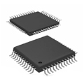
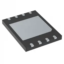
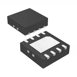
画像は参照用のみです。
TPS22953DSQR
IC PWR SWITCH N-CHAN 1:1 10WSON
- メーカー
- Mfr。パート #TPS22953DSQR
- パッケージ WSON-10
- データシート
- 在庫中4944
100% オリジナル &新しい
出荷の準備ができている24時間
365日の保証
RFQおよびもっと割引を得る
仕様
| Package | Tape & Reel (TR),Cut Tape (CT),Bulk |
| ProductStatus | Active |
| SwitchType | General Purpose |
| NumberofOutputs | 1 |
| Ratio-Input:Output | 1:1 |
| OutputConfiguration | High Side |
| OutputType | N-Channel |
| Interface | On/Off |
| Voltage-Load | 2.5V ~ 5.7V |
| Voltage-Supply(Vcc/Vdd) | Not Required |
| Current-Output(Max) | 5A |
| RdsOn(Typ) | 14mOhm |
| InputType | Non-Inverting |
| Features | Auto Restart, Power Good, Slew Rate Controlled |
| FaultProtection | Over Temperature, Reverse Current, UVLO |
| OperatingTemperature | -40°C ~ 105°C (TA) |
| MountingType | Surface Mount |
| SupplierDevicePackage | 10-WSON (2x2) |
概要
Description
The TPS22953DSQR is a power switch integrated circuit from Texas Instruments, designed for load switching applications. It features a small, compact package ideal for space-constrained designs. The device operates with an input voltage range of 0.6V to 5.7V, making it suitable for a variety of consumer electronics and portable devices.
Key features of the TPS22953DSQR include a controlled turn-on to limit inrush current, minimizing the risk of system damage during startup. It also offers a low ON-resistance, ensuring high efficiency and reduced power loss. The IC includes an integrated controlled output discharge, which helps in discharging the output capacitance during shutdown, thus preventing any undesired voltage residuals.
The TPS22953DSQR supports thermal shutdown and overcurrent protection, enhancing reliability and safety in electronic systems. The device is available in a 2x2mm, 8-pin WSON package, allowing for easy integration into tight board spaces. These features make it an optimal choice for designers looking to manage power distribution efficiently in modern electronic devices.
Key features of the TPS22953DSQR include a controlled turn-on to limit inrush current, minimizing the risk of system damage during startup. It also offers a low ON-resistance, ensuring high efficiency and reduced power loss. The IC includes an integrated controlled output discharge, which helps in discharging the output capacitance during shutdown, thus preventing any undesired voltage residuals.
The TPS22953DSQR supports thermal shutdown and overcurrent protection, enhancing reliability and safety in electronic systems. The device is available in a 2x2mm, 8-pin WSON package, allowing for easy integration into tight board spaces. These features make it an optimal choice for designers looking to manage power distribution efficiently in modern electronic devices.
Features
The TPS22953DSQR is a load switch from Texas Instruments, designed for applications requiring efficient power management and controlled power sequencing. Key features include:
1. Input Voltage Range: Supports an input voltage range of 0.7V to 5.7V, making it versatile for various applications.
2. Current Handling: Capable of handling a continuous current of up to 6A, suitable for high-current load applications.
3. Low On-Resistance: Offers a low on-resistance (R_ON) of approximately 4.7mΩ, ensuring minimal voltage drop and high efficiency.
4. Controlled Rise Time: Provides adjustable slew rate control, allowing for tailored rise times to minimize inrush current.
5. Reverse Current Blocking: Integrated reverse current blocking feature prevents current from flowing back into the power source.
6. Thermal Shutdown: Includes thermal shutdown protection to prevent damage from overheating.
7. Quick Output Discharge (QOD): Ensures output is quickly discharged when the switch is turned off, preventing residual voltage.
8. Package: Comes in a small, space-saving 2mm x 2mm WSON package, suitable for compact designs.
These features make the TPS22953DSQR ideal for use in smartphones, tablets, and other portable electronics where space and efficiency are critical.
1. Input Voltage Range: Supports an input voltage range of 0.7V to 5.7V, making it versatile for various applications.
2. Current Handling: Capable of handling a continuous current of up to 6A, suitable for high-current load applications.
3. Low On-Resistance: Offers a low on-resistance (R_ON) of approximately 4.7mΩ, ensuring minimal voltage drop and high efficiency.
4. Controlled Rise Time: Provides adjustable slew rate control, allowing for tailored rise times to minimize inrush current.
5. Reverse Current Blocking: Integrated reverse current blocking feature prevents current from flowing back into the power source.
6. Thermal Shutdown: Includes thermal shutdown protection to prevent damage from overheating.
7. Quick Output Discharge (QOD): Ensures output is quickly discharged when the switch is turned off, preventing residual voltage.
8. Package: Comes in a small, space-saving 2mm x 2mm WSON package, suitable for compact designs.
These features make the TPS22953DSQR ideal for use in smartphones, tablets, and other portable electronics where space and efficiency are critical.
Package
The TPS22953DSQR is housed in a WSON (Wafer-Level Small Outline No-Lead) package. Specifically, it uses a 10-pin WSON package format, known for its compact and efficient design, ideal for space-constrained applications.
Pinout
The TPS22953DSQR is a load switch from Texas Instruments, typically used for power management in various applications. The package for the TPS22953DSQR is an 8-pin WSON (DSQ) package. Below is a brief description of its pin functions:
1. VIN: Input voltage. Connect to the power source.
2. VOUT: Output voltage. Connect to the load.
3. GND: Ground connection.
4. EN: Enable pin. Used to turn the switch on and off.
5. PG: Power Good indicator. Signals when the output is stable.
6. CT: Capacitor connection. Used to adjust the rise time.
7. NC: Not connected. Reserved for future use or left floating.
8. NC: Another not connected pin.
This configuration supports efficient power management through controlled switching and protection features.
1. VIN: Input voltage. Connect to the power source.
2. VOUT: Output voltage. Connect to the load.
3. GND: Ground connection.
4. EN: Enable pin. Used to turn the switch on and off.
5. PG: Power Good indicator. Signals when the output is stable.
6. CT: Capacitor connection. Used to adjust the rise time.
7. NC: Not connected. Reserved for future use or left floating.
8. NC: Another not connected pin.
This configuration supports efficient power management through controlled switching and protection features.
Manufacturer
The TPS22953DSQR is manufactured by Texas Instruments (TI). Texas Instruments is a global technology company that designs and manufactures semiconductors and various integrated circuits. Their products are used in electronics across a wide range of industries, including automotive, industrial, personal electronics, communications equipment, and enterprise systems. TI is renowned for its innovation in analog and embedded processing products and is a leader in the semiconductor industry.
Application
The TPS22953DSQR is a load switch designed for power management applications. It is commonly used in battery-powered devices, smartphones, tablets, and portable electronics. Its ability to handle high current loads makes it suitable for managing power distribution in these devices. Additionally, it can be used in computing and networking equipment, where efficient power control and distribution are essential. The switch's low ON-resistance and integrated thermal shutdown features make it ideal for applications requiring high efficiency and reliability.
Equivalent
The TPS22953DSQR is a load switch from Texas Instruments. Equivalent products from other manufacturers may include:
1. ON Semiconductor's NCP45560: A similar load switch with comparable voltage and current ratings.
2. Analog Devices' ADP199: An efficient load switch for portable devices.
3. Maxim Integrated's MAX4995: A low-voltage, low-dropout load switch.
When choosing an equivalent, ensure specifications like input voltage, current rating, on-resistance, and package type meet your requirements. Always verify with the latest datasheets for compatibility.
1. ON Semiconductor's NCP45560: A similar load switch with comparable voltage and current ratings.
2. Analog Devices' ADP199: An efficient load switch for portable devices.
3. Maxim Integrated's MAX4995: A low-voltage, low-dropout load switch.
When choosing an equivalent, ensure specifications like input voltage, current rating, on-resistance, and package type meet your requirements. Always verify with the latest datasheets for compatibility.
出荷
出荷方法私たち
DHL、FedEx、TNT、UPS、またはあなたの選択の他の運送業者を通じてグローバルな出荷サービスを提供します。
出荷料参照(DHL/FedEx):
DHL の: 配送費は25ドル〜45ドル(0.5kg)の範囲で、推定配送時間は2〜5営業日です。
フェデックス: 配送費は25ドル〜40ドル(0.5kg)の範囲で、推定配送時間は3〜7営業日。
UPS の: 配送費は25ドル〜45ドル(0.5kg)の範囲で、推定配送時間は3〜7営業日。
TNT社: 配送費は25ドル〜65ドル(0.5kg)の範囲で、推定配送時間は3〜7営業日。
EMS: 配送料金は30〜50ドル(0.5kg)の範囲で、推定配送時間は7〜15営業日です。
登録航空郵便: 配送費は2〜4ドル(0.1kg)で、推定配送時間は5〜20営業日です。
支払い
Payment Methods
支払い期間は100%前払いです。
現在、下記の支払い方法のみを受け入れています。:
1. ペイパル
2. クレジット・デビットカード
3. ワイヤー 転送
類似
-
![MX25R8035FM1IL0]() MX25R8035FM1IL0
Macronix
-
![MX25V1635FZNQ03]() MX25V1635FZNQ03
Macronix
-
![MX29F400CBTI-70G]() MX29F400CBTI-70G
Macronix
-
![MX25V5126FM1I]() MX25V5126FM1I
Macronix
-
![MX25V16066M2I02]() MX25V16066M2I02
Macronix
-
![MX25R6435FBDIL0]() MX25R6435FBDIL0
Macronix
-
![MX25U25643GZNI00]() MX25U25643GZNI00
Macronix
-
![MX25L2006EM1I-12G]() MX25L2006EM1I-12G
Macronix
-
![MX25L6433FM2I-08G]() MX25L6433FM2I-08G
Macronix
-
![MX25L12833FM2I-10G]() MX25L12833FM2I-10..
Macronix
-
![MX25L12833FZ2I-10G]() MX25L12833FZ2I-10..
Macronix
-
![MX25L12833FZNI-10G]() MX25L12833FZNI-10..
Macronix