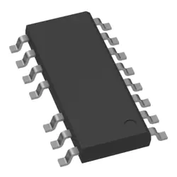
画像は参照用のみです。
TLV62065TDSGRQ1
IC REG BUCK ADJUSTABLE 2A 8WSON
- メーカー
- Mfr。パート #TLV62065TDSGRQ1
- パッケージ 8-WFDFNExposedPad
- データシート
- 在庫中3557
100% オリジナル &新しい
出荷の準備ができている24時間
365日の保証
RFQおよびもっと割引を得る
仕様
| Package | Tape & Reel (TR),Cut Tape (CT) |
| Series | Automotive, AEC-Q100 |
| ProductStatus | Obsolete |
| Function | Step-Down |
| OutputConfiguration | Positive |
| Topology | Buck |
| OutputType | Adjustable |
| NumberofOutputs | 1 |
| Voltage-Input(Min) | 2.9V |
| Voltage-Input(Max) | 5.5V |
| Voltage-Output(Min/Fixed) | 0.8V |
| Voltage-Output(Max) | 5.5V |
| Current-Output | 2A |
| Frequency-Switching | 3MHz |
| SynchronousRectifier | Yes |
| OperatingTemperature | -40°C ~ 105°C (TA) |
| MountingType | Surface Mount |
| Package/Case | 8-WFDFN Exposed Pad |
概要
Description
The TLV62065TDSGRQ1 is a high-efficiency step-down converter by Texas Instruments, designed for automotive applications. It is part of the company's Q1 series, which meets the automotive industry's stringent quality and reliability standards. The device operates over a wide input voltage range and can deliver up to 2A of output current, making it suitable for powering a variety of automotive systems.
Key features of the TLV62065TDSGRQ1 include a wide input voltage range of 2.7V to 5.5V, fixed output voltage options, and a high efficiency of up to 95%. It also incorporates a power-save mode to maintain high efficiency at light loads, and an adjustable output voltage through external resistors. The converter operates at a 2.25 MHz switching frequency, which allows for the use of smaller external components, saving board space.
The TLV62065TDSGRQ1 is available in a 2mm x 2mm WSON package, providing a compact solution for space-constrained applications. Additionally, it features protection mechanisms, such as thermal shutdown and short-circuit protection, ensuring reliable operation in challenging environments. Its automotive-grade performance makes it an ideal choice for battery-powered devices and automotive infotainment systems.
Features
The TLV62065TDSGRQ1 is a step-down converter designed for applications requiring high efficiency and compact size. Key features include:
1. Wide Input Voltage Range: Supports 2.3V to 5.5V, suitable for single-cell Li-Ion battery-powered devices.
2. Output Voltage: Adjustable output voltage range from 0.8V to VIN.
3. Output Current: Delivers up to 2A continuous output current.
4. Efficiency: High efficiency, up to 95%, due to low RDS(ON) power switches.
5. Quiescent Current: Low quiescent current of 17μA, beneficial for battery-powered applications.
6. Switching Frequency: Fixed switching frequency of 2.25 MHz, allowing the use of small inductors and capacitors.
7. Thermal Shutdown: Integrated thermal protection feature to prevent damage due to overheating.
8. Soft Start and Enable Pin: Built-in soft start and an enable pin for easy power management.
9. Package: Comes in a small 8-pin WSON package, aiding in compact PCB designs.
10. Automotive Grade: AEC-Q100 qualified, making it suitable for automotive applications.
These features make the TLV62065TDSGRQ1 ideal for various applications, including portable electronics, automotive systems, and industrial products requiring efficient power management.
Package
The TLV62065TDSGRQ1 is a step-down converter from Texas Instruments. It is available in a small 2 mm x 3 mm, 8-pin WSON (DSG) package, which is suitable for compact applications.
Pinout
The TLV62065TDSGRQ1 is an automotive-qualified, high-efficiency step-down DC-DC converter. It is designed for portable and automotive applications and is manufactured by Texas Instruments.
The device comes in an 8-pin WSON (DSG) package. The pin functions are as follows:
1. EN (Enable): This pin enables or disables the device. A high level turns the device on, while a low level turns it off.
2. VIN (Input Voltage): This pin is the input supply voltage.
3. SW (Switch): This pin is the switch node, connected to the inductor.
4. GND (Ground): This is the ground reference for the device.
5. FB (Feedback): This pin is used to set the output voltage via an external resistor divider.
6. VOS (Output Voltage Sense): This pin senses the output voltage for regulation.
7. PG (Power Good): This pin indicates the output voltage status.
8. SS/TR (Soft Start/Tracking): This pin is used for soft start and tracking applications.
This configuration allows the TLV62065TDSGRQ1 to provide efficient power conversion with precise output voltage regulation.
Manufacturer
The TLV62065TDSGRQ1 is manufactured by Texas Instruments. Texas Instruments (TI) is an American technology company known for designing and manufacturing semiconductors and various integrated circuits. These products are used in a broad range of electronic applications, including consumer electronics, automotive systems, industrial equipment, and communication devices. TI is one of the world’s largest semiconductor companies and is well-regarded for its innovation and contributions to the electronics industry.
Application
The TLV62065TDSGRQ1 is a DC-DC step-down converter commonly used in automotive applications due to its AEC-Q100 qualification. It is suitable for powering microcontrollers, sensors, and other electronic components requiring a stable voltage supply in automotive systems. Additionally, its compact size and efficiency make it ideal for battery-powered devices and portable electronics where space and power efficiency are crucial.
Equivalent
The TLV62065TDSGRQ1 is a step-down DC-DC converter from Texas Instruments. Equivalent products from other manufacturers include:
1. Microchip Technology: MCP16301
2. ON Semiconductor: NCP1529
3. Analog Devices: ADP2300
4. Maxim Integrated: MAX16903
These alternatives offer similar functionalities in terms of voltage regulation and efficiency but may differ slightly in features or specifications. Always check the datasheet for compatibility with your specific application.
出荷
出荷方法私たち
DHL、FedEx、TNT、UPS、またはあなたの選択の他の運送業者を通じてグローバルな出荷サービスを提供します。
出荷料参照(DHL/FedEx):
DHL の: 配送費は25ドル〜45ドル(0.5kg)の範囲で、推定配送時間は2〜5営業日です。
フェデックス: 配送費は25ドル〜40ドル(0.5kg)の範囲で、推定配送時間は3〜7営業日。
UPS の: 配送費は25ドル〜45ドル(0.5kg)の範囲で、推定配送時間は3〜7営業日。
TNT社: 配送費は25ドル〜65ドル(0.5kg)の範囲で、推定配送時間は3〜7営業日。
EMS: 配送料金は30〜50ドル(0.5kg)の範囲で、推定配送時間は7〜15営業日です。
登録航空郵便: 配送費は2〜4ドル(0.1kg)で、推定配送時間は5〜20営業日です。
支払い
Payment Methods
支払い期間は100%前払いです。
現在、下記の支払い方法のみを受け入れています。:
1. ペイパル
2. クレジット・デビットカード
3. ワイヤー 転送
類似
-
![MX29F400CBTI-70G]() MX29F400CBTI-70G
Macronix
-
![MX25V4035FZUI]() MX25V4035FZUI
Macronix
-
![MX25V2033FM1I]() MX25V2033FM1I
Macronix
-
![MX25R3235FZNIL0]() MX25R3235FZNIL0
Macronix
-
![MX25V16066M2I02]() MX25V16066M2I02
Macronix
-
![MX25L25673GMI-08G]() MX25L25673GMI-08G
Macronix
-
![MX25L2006EM1I-12G]() MX25L2006EM1I-12G
Macronix
-
![MX25U6435FM2I-10G]() MX25U6435FM2I-10G
Macronix
-
![MX25L12835FZ2I-10G]() MX25L12835FZ2I-10..
Macronix
-
![MX29F800CBTI-70G]() MX29F800CBTI-70G
Macronix
-
![MX29LV640ETTI-70G]() MX29LV640ETTI-70G
Macronix
-
![MX25L25735FMI-10G]() MX25L25735FMI-10G
Macronix