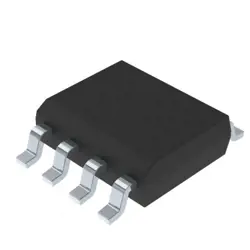
画像は参照用のみです。
TC7S14FU
- メーカー
- Mfr。パート #TC7S14FU
- パッケージ
- データシート
- 在庫中6834
100% オリジナル &新しい
出荷の準備ができている24時間
365日の保証
RFQおよびもっと割引を得る
仕様
| Series | TC7S14 |
| Brand | Toshiba |
| Product Type | Inverters |
| Subcategory | Logic ICs |
| Logic Family | S |
概要
Description
The TC7S14FU is a logic gate integrated circuit produced by Toshiba. It is a CMOS (Complementary Metal-Oxide-Semiconductor) device, notable for its low power consumption and high noise immunity. Specifically, the TC7S14FU is an inverter, which means it outputs the opposite logical state to its input; if the input is high (logic 1), the output is low (logic 0), and vice versa. It operates over a wide voltage range, typically from 2V to 5.5V, making it versatile for various digital logic applications.
The device is housed in a small, flat-lead packaging, making it suitable for compact circuit designs. Its fast switching speed and low quiescent current are advantageous for mobile and battery-powered applications. The TC7S14FU is commonly used in digital circuits for tasks such as signal inversion, logic level conversion, and timing applications. Its robust design ensures reliable performance in various environmental conditions.
The device is housed in a small, flat-lead packaging, making it suitable for compact circuit designs. Its fast switching speed and low quiescent current are advantageous for mobile and battery-powered applications. The TC7S14FU is commonly used in digital circuits for tasks such as signal inversion, logic level conversion, and timing applications. Its robust design ensures reliable performance in various environmental conditions.
Features
The TC7S14FU is a single Schmitt inverter, which is a type of logic gate used in digital circuits. Here are some key features:
1. Schmitt Trigger Action: It provides a built-in hysteresis between the positive-going and negative-going input threshold voltages, enhancing noise immunity and producing clean output signals for slower or noisy input transitions.
2. Single Gate Inverter: The device functions as an inverter, meaning it outputs the opposite logic level of its input signal.
3. Wide Operating Voltage Range: Typically operates in a wide voltage range, often from about 2V to 5.5V, making it suitable for various applications.
4. Low Power Consumption: It is designed to consume minimal power, which is ideal for battery-operated devices.
5. Fast Switching Speed: Offers quick transition times, improving performance in high-speed applications.
6. Compact Package: Often available in small, surface-mount packages, making it suitable for compact designs.
7. High Noise Immunity: The Schmitt trigger design allows for robust performance even in environments with electrical noise.
These features make the TC7S14FU suitable for applications requiring simple signal inversion with enhanced noise immunity and low power usage.
Package
The TC7S14FU is housed in a surface-mount package type known as SSOP5 (Shrink Small Outline Package with 5 leads). This compact package is commonly used for space-efficient applications in electronic circuits.
Pinout
The TC7S14FU is a single Schmitt-trigger inverter from Toshiba. It is a small, surface-mount device typically housed in a SOT-353 package. The device has a pin count of 5. Here is a brief overview of its pin functions:
1. Pin 1 (A): Input pin for the Schmitt-trigger inverter.
2. Pin 2 (GND): Ground connection for the circuit.
3. Pin 3 (Y): Output pin of the inverter.
4. Pin 4 (NC): No connection, often not used.
5. Pin 5 (VCC): Supply voltage for the device.
The TC7S14FU is designed to provide a stable output even in the presence of slow input signal transitions, thus aiding in noise immunity and signal stabilization. It is widely used in digital circuits where an inversion function with Schmitt-trigger action is required.
Manufacturer
The TC7S14FU is manufactured by Toshiba Electronic Devices & Storage Corporation, which is a part of the Toshiba Corporation. Toshiba is a multinational conglomerate headquartered in Japan, known for its diversified range of products and services including electronics, electrical equipment, and information technology. The company is well-regarded for its technological innovations and plays a significant role in various sectors such as semiconductors, storage devices, and infrastructure systems.
Application
The TC7S14FU is a single Schmitt inverter IC commonly used in applications requiring signal conditioning, noise elimination, and waveform shaping. Its primary use is in digital circuits to convert noisy or slow input signals into clean, fast digital outputs. This makes it suitable for use in signal processing, communication systems, and as a buffer or driver in power-sensitive devices. Additionally, its low power consumption makes it ideal for battery-operated applications.
Equivalent
The TC7S14FU is a Schmitt trigger inverter. Equivalent products include the 74LVC1G14, 74HC1G14, and SN74LVC1G14 chips, which are typically offered by manufacturers like Texas Instruments, Nexperia, and ON Semiconductor. Always check the specific datasheets to verify compatibility in terms of voltage, speed, and other characteristics.
出荷
出荷方法私たち
DHL、FedEx、TNT、UPS、またはあなたの選択の他の運送業者を通じてグローバルな出荷サービスを提供します。
出荷料参照(DHL/FedEx):
DHL の: 配送費は25ドル〜45ドル(0.5kg)の範囲で、推定配送時間は2〜5営業日です。
フェデックス: 配送費は25ドル〜40ドル(0.5kg)の範囲で、推定配送時間は3〜7営業日。
UPS の: 配送費は25ドル〜45ドル(0.5kg)の範囲で、推定配送時間は3〜7営業日。
TNT社: 配送費は25ドル〜65ドル(0.5kg)の範囲で、推定配送時間は3〜7営業日。
EMS: 配送料金は30〜50ドル(0.5kg)の範囲で、推定配送時間は7〜15営業日です。
登録航空郵便: 配送費は2〜4ドル(0.1kg)で、推定配送時間は5〜20営業日です。
支払い
Payment Methods
支払い期間は100%前払いです。
現在、下記の支払い方法のみを受け入れています。:
1. ペイパル
2. クレジット・デビットカード
3. ワイヤー 転送
類似
-
![MX25V1635FZNI]() MX25V1635FZNI
Macronix
-
![MX25L8035EM2I-10G]() MX25L8035EM2I-10G
Macronix
-
![MX25L25673GMI-10G]() MX25L25673GMI-10G
Macronix
-
![MX25U25643GZNI00]() MX25U25643GZNI00
Macronix
-
![MX25V1635FM2I]() MX25V1635FM2I
Macronix
-
![MX25L12833FM2I-10G]() MX25L12833FM2I-10..
Macronix
-
![MX25U25645GXDI00]() MX25U25645GXDI00
Macronix
-
![MX25L12835FZ2I-10G]() MX25L12835FZ2I-10..
Macronix
-
![MX29LV160DTTI-70G]() MX29LV160DTTI-70G
Macronix
-
![MX29F040CTI-70G]() MX29F040CTI-70G
Macronix
-
![MX29LV640ETTI-70G]() MX29LV640ETTI-70G
Macronix
-
![MX25L1006EMI-10G]() MX25L1006EMI-10G
Macronix