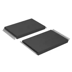
画像は参照用のみです。
TC7660EOA
IC REG CHARG PUMP INV 20MA 8SOIC
- メーカー
- Mfr。パート #TC7660EOA
- パッケージ 8-SOIC
- データシート TC7660EOA DataSheet
- 在庫中5523
100% オリジナル &新しい
出荷の準備ができている24時間
365日の保証
RFQおよびもっと割引を得る
仕様
| Package | Tube |
| ProductStatus | Active |
| Function | Ratiometric |
| OutputConfiguration | Positive or Negative |
| Topology | Charge Pump |
| OutputType | Fixed |
| NumberofOutputs | 1 |
| Voltage-Input(Min) | 1.5V |
| Voltage-Input(Max) | 10V |
| Voltage-Output(Min/Fixed) | -Vin, 2Vin |
| Current-Output | 20mA |
| Frequency-Switching | 10kHz |
| SynchronousRectifier | No |
| OperatingTemperature | -40°C ~ 85°C (TA) |
| MountingType | Surface Mount |
| Package/Case | 8-SOIC (0.154, 3.90mm Width) |
概要
Description
The TC7660EOA is a charge pump voltage converter integrated circuit (IC) designed to invert the input voltage, commonly used in applications where a negative voltage is required from a positive supply. It operates on a wide input voltage range, typically between 1.5V and 10V, making it versatile for various electronic applications. The device efficiently converts a positive input voltage to a corresponding negative output voltage, approximately equal in magnitude to the input.
Key features of the TC7660EOA include low supply current, typically around 80µA, and the ability to deliver up to 20mA of output current, depending on the input voltage. It has a high conversion efficiency, usually around 95%, and minimal external components are needed, often just two capacitors. The IC is suitable for use in battery-operated devices, operational amplifier circuits, and other low-power applications.
The TC7660EOA is housed in a compact 8-pin SOIC package, which is advantageous for space-constrained designs. Its ease of use and reliability make it a popular choice for designers looking to implement simple and efficient voltage inversion in their projects.
Features
The TC7660EOA is a charge pump voltage converter IC designed to invert input voltages. Key features include:
1. Voltage Range: Operates with input voltages from 1.5V to 10V.
2. Output: Provides inverted output voltage, approximately -Vin.
3. Low Quiescent Current: Consumes minimal power in idle mode, improving efficiency.
4. Conversion Efficiency: Up to 98% efficiency, thanks to its switched-capacitor architecture.
5. Compact Design: Available in small, surface-mount packages like SOIC-8, making it suitable for space-constrained applications.
6. Operating Temperature: Functions reliably within a wide temperature range, typically -40°C to +85°C.
7. Easy Implementation: Requires few external components, simplifying design and reducing overall system cost.
8. No Inductors: The design eliminates the need for inductors, minimizing electromagnetic interference.
9. Applications: Ideal for battery-powered devices, data acquisition systems, dual-supply systems, and any application needing a negative voltage.
Overall, the TC7660EOA is a versatile component ideal for efficient and compact power supply designs.
Package
The TC7660EOA is available in an 8-pin SOIC (Small Outline Integrated Circuit) package.
Pinout
The TC7660EOA is a voltage converter IC commonly used for generating a negative voltage from a positive supply voltage. This IC typically comes in an 8-pin configuration. Here is a brief overview of its pin functions:
1. Pin 1 (CAP+): Positive terminal for the charge-pump capacitor. Connect this pin to one terminal of the external capacitor used for the charge pump.
2. Pin 2 (GND): Ground reference point. Connect this to the ground of the circuit.
3. Pin 3 (CAP-): Negative terminal for the charge-pump capacitor. Connect this to the other terminal of the external charge-pump capacitor.
4. Pin 4 (VOUT): Output voltage pin. This pin provides the inverted voltage output.
5. Pin 5 (LV): Low-voltage operation pin. Used to optimize performance for low input voltages; it can be connected to V+ for normal operation.
6. Pin 6 (OSC): Oscillator control pin. It can be used to adjust the oscillator frequency if necessary.
7. Pin 7 (V+): Positive supply voltage pin. Connect this to the positive side of the supply voltage.
8. Pin 8 (NC): No connection, typically left unconnected or used for mechanical stability.
The TC7660EOA effectively doubles the negative voltage, making it suitable for applications requiring a simple charge-pump voltage inverter.
Manufacturer
The TC7660EOA is manufactured by Microchip Technology Inc. Microchip is a leading semiconductor company that designs and produces microcontrollers, mixed-signal, analog, and Flash-IP integrated circuits. The company serves a wide range of applications across the industrial, automotive, consumer, aerospace, and communications markets. Microchip is known for its focus on providing high-quality and reliable solutions to its customers, enabling innovation and efficiency in electronic design.
Application
The TC7660EOA is a charge pump voltage converter used in applications requiring a negative voltage supply. Common areas include biasing analog circuits, LCDs, sensors, and operational amplifiers where a negative voltage is necessary. It's also used in battery-powered devices, providing efficient voltage inversion with minimal external components, making it suitable for portable and compact electronic devices.
Equivalent
The TC7660EOA is a charge pump voltage converter. Equivalent products include the ICL7660, MAX1044, LTC1044, LM2660, and MC7660. These are all inverters or voltage doublers with similar specifications and pin configurations, suitable for generating negative voltage from a positive voltage supply. Always check the datasheet for each to ensure compatibility with your specific application requirements.
出荷
出荷方法私たち
DHL、FedEx、TNT、UPS、またはあなたの選択の他の運送業者を通じてグローバルな出荷サービスを提供します。
出荷料参照(DHL/FedEx):
DHL の: 配送費は25ドル〜45ドル(0.5kg)の範囲で、推定配送時間は2〜5営業日です。
フェデックス: 配送費は25ドル〜40ドル(0.5kg)の範囲で、推定配送時間は3〜7営業日。
UPS の: 配送費は25ドル〜45ドル(0.5kg)の範囲で、推定配送時間は3〜7営業日。
TNT社: 配送費は25ドル〜65ドル(0.5kg)の範囲で、推定配送時間は3〜7営業日。
EMS: 配送料金は30〜50ドル(0.5kg)の範囲で、推定配送時間は7〜15営業日です。
登録航空郵便: 配送費は2〜4ドル(0.1kg)で、推定配送時間は5〜20営業日です。
支払い
Payment Methods
支払い期間は100%前払いです。
現在、下記の支払い方法のみを受け入れています。:
1. ペイパル
2. クレジット・デビットカード
3. ワイヤー 転送
類似
-
![MX25R8035FM1IL0]() MX25R8035FM1IL0
Macronix
-
![MX25V1635FZNQ03]() MX25V1635FZNQ03
Macronix
-
![MX66U1G45GXDI00]() MX66U1G45GXDI00
Macronix
-
![MX25V5126FM1I]() MX25V5126FM1I
Macronix
-
![MX25R6435FBDIL0]() MX25R6435FBDIL0
Macronix
-
![MX25L25673GMI-10G]() MX25L25673GMI-10G
Macronix
-
![MX25U25645GXDI00]() MX25U25645GXDI00
Macronix
-
![MX25L12835FZ2I-10G]() MX25L12835FZ2I-10..
Macronix
-
![MX29F040CTI-70G]() MX29F040CTI-70G
Macronix
-
![MX29F800CBTI-70G]() MX29F800CBTI-70G
Macronix
-
![MX29LV640ETTI-70G]() MX29LV640ETTI-70G
Macronix
-
![MX25L1006EMI-10G]() MX25L1006EMI-10G
Macronix