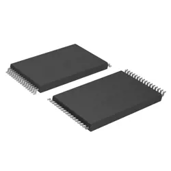
画像は参照用のみです。
TC54VC2102ECB713
IC SUPERVISOR 1 CHANNEL SOT23A-3
- メーカー
- Mfr。パート #TC54VC2102ECB713
- パッケージ TO-236-3, SC-59, SOT-23-3
- データシート TC54VC2102ECB713 DataSheet
- 在庫中4862
100% オリジナル &新しい
出荷の準備ができている24時間
365日の保証
RFQおよびもっと割引を得る
仕様
| Package | Tape & Reel (TR),Cut Tape (CT) |
| ProductStatus | Active |
| Type | Simple Reset/Power-On Reset |
| NumberofVoltagesMonitored | 1 |
| Voltage-Threshold | 2.1V |
| Output | Push-Pull, Totem Pole |
| Reset | Active Low |
| OperatingTemperature | -40°C ~ 85°C (TA) |
| MountingType | Surface Mount |
| Package/Case | TO-236-3, SC-59, SOT-23-3 |
概要
Description
The TC54VC2102ECB713 is a Toshiba static RAM (SRAM) device in the TC54VC family. It provides small, fast, volatile memory for buffering and caching in embedded systems.
Key points:
- Capacity and type: typically 1K × 8 bits (1024 × 8) SRAM, not non-volatile.
- Voltage and signaling: VC indicates a low‑voltage CMOS SRAM variant (commonly 2.7–3.6 V operation).
- Interface: asynchronous memory with 10 address lines (A0–A9), 8 data I/O lines (DQ0–DQ7), and standard control pins—Chip Enable (CE), Output Enable (OE), and Write Enable (WE).
- Operation: read when CE and OE are asserted (OE active, WE inactive); write when CE and WE are asserted (OE ignored during write). Outputs are tri‑stated when CE is deasserted.
- Packaging: ECB713 marking indicates a Pb-free package variant; exact package type shown in datasheet.
Uses: general-purpose RAM for microcontroller buffers, caches, data tables, and other small, fast storage needs.
Note: For exact electrical specs (access time, power, standby current) and pinout, refer to the official TC54VC2102ECB713 datasheet.
Key points:
- Capacity and type: typically 1K × 8 bits (1024 × 8) SRAM, not non-volatile.
- Voltage and signaling: VC indicates a low‑voltage CMOS SRAM variant (commonly 2.7–3.6 V operation).
- Interface: asynchronous memory with 10 address lines (A0–A9), 8 data I/O lines (DQ0–DQ7), and standard control pins—Chip Enable (CE), Output Enable (OE), and Write Enable (WE).
- Operation: read when CE and OE are asserted (OE active, WE inactive); write when CE and WE are asserted (OE ignored during write). Outputs are tri‑stated when CE is deasserted.
- Packaging: ECB713 marking indicates a Pb-free package variant; exact package type shown in datasheet.
Uses: general-purpose RAM for microcontroller buffers, caches, data tables, and other small, fast storage needs.
Note: For exact electrical specs (access time, power, standby current) and pinout, refer to the official TC54VC2102ECB713 datasheet.
Package
Cannot determine the package type from the part number alone. Please refer to the official datasheet or product page for TC54VC2102ECB713 to confirm the exact package (e.g., LQFP, TSSOP, BGA) and pin count.
Pinout
Pin count: 16 pins.
Function: Dual-channel bidirectional voltage-level translator (logic-level shifter) used to translate signals between different supply-voltage domains.
Function: Dual-channel bidirectional voltage-level translator (logic-level shifter) used to translate signals between different supply-voltage domains.
Manufacturer
Manufacturer: Toshiba (specifically Toshiba Electronics Devices & Storage Corporation).
What kind of company: A Japanese multinational conglomerate and one of the world’s leading producers of electronics and semiconductors (memory, power devices, sensors, etc.).
What kind of company: A Japanese multinational conglomerate and one of the world’s leading producers of electronics and semiconductors (memory, power devices, sensors, etc.).
Application
Possible application areas for TC54VC2102ECB713 (voltage level translator):
- Mixed‑voltage level shifting (e.g., 1.8V to 3.3V/5V)
- Bidirectional I2C/SPI/UART bus translation
- Interfaces between microcontrollers, sensors, memories, and peripherals at different logic levels
- Portable/embedded devices and wearables
- Automotive and industrial electronics signal interfacing
- General data‑bus bridging and interface protection in consumer electronics
Note: refer to the datasheet for exact capabilities and pinout.
- Mixed‑voltage level shifting (e.g., 1.8V to 3.3V/5V)
- Bidirectional I2C/SPI/UART bus translation
- Interfaces between microcontrollers, sensors, memories, and peripherals at different logic levels
- Portable/embedded devices and wearables
- Automotive and industrial electronics signal interfacing
- General data‑bus bridging and interface protection in consumer electronics
Note: refer to the datasheet for exact capabilities and pinout.
出荷
出荷方法私たち
DHL、FedEx、TNT、UPS、またはあなたの選択の他の運送業者を通じてグローバルな出荷サービスを提供します。
出荷料参照(DHL/FedEx):
DHL の: 配送費は25ドル〜45ドル(0.5kg)の範囲で、推定配送時間は2〜5営業日です。
フェデックス: 配送費は25ドル〜40ドル(0.5kg)の範囲で、推定配送時間は3〜7営業日。
UPS の: 配送費は25ドル〜45ドル(0.5kg)の範囲で、推定配送時間は3〜7営業日。
TNT社: 配送費は25ドル〜65ドル(0.5kg)の範囲で、推定配送時間は3〜7営業日。
EMS: 配送料金は30〜50ドル(0.5kg)の範囲で、推定配送時間は7〜15営業日です。
登録航空郵便: 配送費は2〜4ドル(0.1kg)で、推定配送時間は5〜20営業日です。
支払い
Payment Methods
支払い期間は100%前払いです。
現在、下記の支払い方法のみを受け入れています。:
1. ペイパル
2. クレジット・デビットカード
3. ワイヤー 転送
類似
-
![MX25V5126FM1I]() MX25V5126FM1I
Macronix
-
![MX25V4035FZUI]() MX25V4035FZUI
Macronix
-
![MX25R6435FBDIL0]() MX25R6435FBDIL0
Macronix
-
![MX25U51279GXDR00]() MX25U51279GXDR00
Macronix
-
![MX25V1635FM2I]() MX25V1635FM2I
Macronix
-
![MX25U3232FZBI02]() MX25U3232FZBI02
Macronix
-
![MX25L6433FM2I-08G]() MX25L6433FM2I-08G
Macronix
-
![MX25U6435FM2I-10G]() MX25U6435FM2I-10G
Macronix
-
![MX25U25645GXDI00]() MX25U25645GXDI00
Macronix
-
![MX25L12835FZ2I-10G]() MX25L12835FZ2I-10..
Macronix
-
![MX25L25645GXDI-08G]() MX25L25645GXDI-08..
Macronix
-
![MX29F040CTI-70G]() MX29F040CTI-70G
Macronix