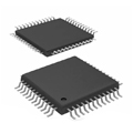
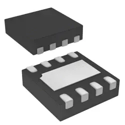
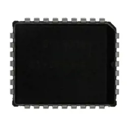
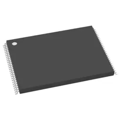
画像は参照用のみです。
SY89838UMG
IC CLK BUFFER 2:8 2GHZ 32QFN
- メーカー
- Mfr。パート #SY89838UMG
- パッケージ
- データシート SY89838UMG DataSheet
- 在庫中3882
100% オリジナル &新しい
出荷の準備ができている24時間
365日の保証
RFQおよびもっと割引を得る
仕様
| Series | Precision Edge® |
| Part Status | Active |
| Type | Fanout Buffer (Distribution), Multiplexer |
| Number of Circuits | 1 |
| Ratio - Input:Output | 2:8 |
| Differential - Input:Output | Yes/Yes |
| Input | CML, LVDS, LVPECL |
| Output | LVDS |
| Frequency - Max | 2 GHz |
| Voltage - Supply | 2.375V ~ 2.625V |
| Operating Temperature | -40°C ~ 85°C |
| Mounting Type | Surface Mount |
| Package / Case | 32-VFQFN Exposed Pad |
| Supplier Device Package | 32-QFN (5x5) |
| Base Product Number | SY89838 |
概要
Description
The SY89838UMG is a high-performance differential clock and data distribution device designed by Microchip Technology. It is optimized for applications requiring low skew and high fidelity in signal transmission, making it ideal for use in high-speed communication systems, such as data centers and telecom equipment.
Key features include a wide input frequency range, support for multiple output configurations, and low propagation delay, which ensures minimal signal distortion. The device typically includes integrated voltage level shifting and can support single-ended or differential outputs, enhancing its versatility in various circuit designs.
In terms of power consumption, the SY89838UMG is designed to operate efficiently, contributing to overall system performance while maintaining thermal management standards. It is often used in conjunction with other components in a system to ensure reliable and synchronized operation across multiple channels.
Overall, the SY89838UMG is a valuable component for engineers looking to improve data integrity and speed in their designs.
Key features include a wide input frequency range, support for multiple output configurations, and low propagation delay, which ensures minimal signal distortion. The device typically includes integrated voltage level shifting and can support single-ended or differential outputs, enhancing its versatility in various circuit designs.
In terms of power consumption, the SY89838UMG is designed to operate efficiently, contributing to overall system performance while maintaining thermal management standards. It is often used in conjunction with other components in a system to ensure reliable and synchronized operation across multiple channels.
Overall, the SY89838UMG is a valuable component for engineers looking to improve data integrity and speed in their designs.
Features
The SY89838UMG is a high-speed, low-jitter clock and data recovery device from Synergy Microwave Corporation, designed for applications demanding precise timing and synchronization. Key features include:
1. High-Speed Operation: Supports data rates up to 3.2 Gbps, making it suitable for high-performance communication systems.
2. Low Jitter: Offers ultra-low jitter performance, critical for maintaining signal integrity in high-speed applications.
3. Versatile Input/Output: Accepts differential input signals and provides multiple output configurations, catering to diverse system requirements.
4. Integrated Phase-Locked Loop (PLL): Features a built-in PLL for improved clock recovery and synchronization.
5. Wide Supply Voltage Range: Operates within a broad voltage range, enhancing flexibility for various electronic designs.
6. Compact Package: Available in a small footprint, facilitating integration into space-constrained environments.
These features make the SY89838UMG ideal for networking, telecommunications, and other high-speed digital applications.
1. High-Speed Operation: Supports data rates up to 3.2 Gbps, making it suitable for high-performance communication systems.
2. Low Jitter: Offers ultra-low jitter performance, critical for maintaining signal integrity in high-speed applications.
3. Versatile Input/Output: Accepts differential input signals and provides multiple output configurations, catering to diverse system requirements.
4. Integrated Phase-Locked Loop (PLL): Features a built-in PLL for improved clock recovery and synchronization.
5. Wide Supply Voltage Range: Operates within a broad voltage range, enhancing flexibility for various electronic designs.
6. Compact Package: Available in a small footprint, facilitating integration into space-constrained environments.
These features make the SY89838UMG ideal for networking, telecommunications, and other high-speed digital applications.
Package
The SY89838UMG is offered in a 16-pin TQFN (Thin Quad Flat No-lead) package. This compact package design is suitable for high-performance applications, providing efficient thermal management and space-saving benefits.
Pinout
The SY89838UMG is a high-speed, low-power Differential Precision Clock Driver with a pin count of 16.
Pin Functions:
1. VCC: Power supply.
2. GND: Ground connection.
3. OUT_A, OUT_B: Differential output pairs for clock signals.
4. OUT_A_BAR, OUT_B_BAR: Inverted differential outputs.
5. IN: Differential clock input.
6. IN_BAR: Inverted differential clock input.
7. SEL: Selects the output configuration.
8. I/O: Input/output mode configuration.
9. SLEEP: Sleep mode control.
10. NC: No connection (not used).
The device is designed for applications requiring low skew and high signal integrity, making it suitable for clock distribution in high-performance systems.
Pin Functions:
1. VCC: Power supply.
2. GND: Ground connection.
3. OUT_A, OUT_B: Differential output pairs for clock signals.
4. OUT_A_BAR, OUT_B_BAR: Inverted differential outputs.
5. IN: Differential clock input.
6. IN_BAR: Inverted differential clock input.
7. SEL: Selects the output configuration.
8. I/O: Input/output mode configuration.
9. SLEEP: Sleep mode control.
10. NC: No connection (not used).
The device is designed for applications requiring low skew and high signal integrity, making it suitable for clock distribution in high-performance systems.
Manufacturer
The SY89838UMG is manufactured by Synopsys, Inc., a leading company in the electronic design automation (EDA) industry. Synopsys specializes in software and tools for semiconductor design, verification, and manufacturing. The company provides solutions that enable engineers to design and test integrated circuits and systems on chips (SoCs) efficiently. It also offers services related to IP (intellectual property) design, ensuring that its clients can develop high-performance, reliable electronic products. Synopsys is known for its innovation in digital and mixed-signal circuit design, making it a key player in the technology sector.
Application
The SY89838UMG is a high-speed comparator used in various applications, including high-performance data communication systems, clock and data recovery circuits, high-speed serial link systems, and precision analog-to-digital converter (ADC) interfaces. Its low propagation delay and high bandwidth make it suitable for use in telecom, networking, and optical data transmission systems.
Equivalent
The SY89838UMG is a high-speed comparator. Equivalent products include the MAX9000 series from Maxim Integrated, the LTC6752 from Analog Devices, and the LMH6629 from Texas Instruments. Always verify specifications, such as bandwidth, voltage levels, and packaging, to ensure compatibility for your specific application.
出荷
出荷方法私たち
DHL、FedEx、TNT、UPS、またはあなたの選択の他の運送業者を通じてグローバルな出荷サービスを提供します。
出荷料参照(DHL/FedEx):
DHL の: 配送費は25ドル〜45ドル(0.5kg)の範囲で、推定配送時間は2〜5営業日です。
フェデックス: 配送費は25ドル〜40ドル(0.5kg)の範囲で、推定配送時間は3〜7営業日。
UPS の: 配送費は25ドル〜45ドル(0.5kg)の範囲で、推定配送時間は3〜7営業日。
TNT社: 配送費は25ドル〜65ドル(0.5kg)の範囲で、推定配送時間は3〜7営業日。
EMS: 配送料金は30〜50ドル(0.5kg)の範囲で、推定配送時間は7〜15営業日です。
登録航空郵便: 配送費は2〜4ドル(0.1kg)で、推定配送時間は5〜20営業日です。
支払い
Payment Methods
支払い期間は100%前払いです。
現在、下記の支払い方法のみを受け入れています。:
1. ペイパル
2. クレジット・デビットカード
3. ワイヤー 転送
類似
-
![MX25V1635FZNI]() MX25V1635FZNI
Macronix
-
![MX25V1635FZNQ03]() MX25V1635FZNQ03
Macronix
-
![MX66U1G45GXDI00]() MX66U1G45GXDI00
Macronix
-
![MX25V5126FM1I]() MX25V5126FM1I
Macronix
-
![MX25V16066M2I02]() MX25V16066M2I02
Macronix
-
![MX30LF2G28AD-TI]() MX30LF2G28AD-TI
Macronix
-
![MX25R6435FBDIL0]() MX25R6435FBDIL0
Macronix
-
![MX25U3232FZBI02]() MX25U3232FZBI02
Macronix
-
![MX25L12833FM2I-10G]() MX25L12833FM2I-10..
Macronix
-
![MX29F040CQI-70G]() MX29F040CQI-70G
Macronix
-
![MX29F800CBTI-70G]() MX29F800CBTI-70G
Macronix
-
![MX29LV640ETTI-70G]() MX29LV640ETTI-70G
Macronix