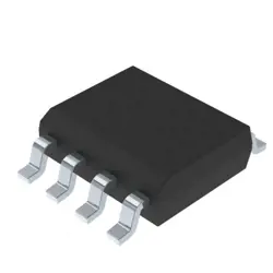
画像は参照用のみです。
SUM55P06-19L-E3
MOSFET P-CH 60V 55A TO263
- メーカー
- Mfr。パート #SUM55P06-19L-E3
- パッケージ
- データシート SUM55P06-19L-E3 DataSheet
- 在庫中5164
100% オリジナル &新しい
出荷の準備ができている24時間
365日の保証
RFQおよびもっと割引を得る
仕様
| Series | TrenchFET® |
| Part Status | Active |
| FET Type | P-Channel |
| Technology | MOSFET (Metal Oxide) |
| Drain to Source Voltage (Vdss) | 60 V |
| Current - Continuous Drain (Id) @ 25°C | 55A (Tc) |
| Drive Voltage (Max Rds On, Min Rds On) | 4.5V, 10V |
| Rds On (Max) @ Id, Vgs | 19mOhm @ 30A, 10V |
| Vgs(th) (Max) @ Id | 3V @ 250µA |
| Gate Charge (Qg) (Max) @ Vgs | 115 nC @ 10 V |
| Vgs (Max) | ±20V |
| Input Capacitance (Ciss) (Max) @ Vds | 3500 pF @ 25 V |
| Power Dissipation (Max) | 3.75W (Ta), 125W (Tc) |
| Operating Temperature | -55°C ~ 175°C (TJ) |
| Mounting Type | Surface Mount |
| Supplier Device Package | TO-263 (D2PAK) |
| Package / Case | TO-263-3, D2PAK (2 Leads + Tab), TO-263AB |
| Base Product Number | SUM55 |
概要
Description
SUM55P06-19L-E3 is a human antibody that targets the protein SUMO-1 (Small Ubiquitin-like Modifier 1). This antibody is designed for use in various research applications, including Western blotting, immunohistochemistry, and flow cytometry. It is significant for studying protein modification processes, particularly in the context of post-translational modifications, which play a crucial role in cellular signaling and regulation. The SUMOylation process, mediated by SUMO proteins, affects various cellular functions, including transcription, DNA repair, and stress responses. SUM55P06-19L-E3 may be utilized in studies aimed at understanding diseases related to SUMO malfunction, such as cancer and neurodegenerative disorders. Researchers often employ this antibody to investigate the dynamics of SUMOylation in different biological contexts.
Features
The SUM55P06-19L-E3 is a power MOSFET designed for high-efficiency applications. Key features include:
1. Type: N-channel MOSFET.
2. Voltage Rating: Supports a maximum drain-source voltage (VDS) of 55V.
3. Current Rating: Capable of handling continuous drain current (ID) up to 80A with appropriate thermal management.
4. RDS(on): Low on-resistance (typically around 10 mΩ), which minimizes conduction losses.
5. Package: Offered in a TO-220 package for efficient heat dissipation and easier mounting.
6. Gate Threshold Voltage: Provides a gate-source threshold voltage (VGS(th)) typically between 1-2V, allowing for easy driving.
7. Applications: Suitable for use in power supplies, motor drivers, and various switching applications.
This MOSFET is ideal for both automotive and industrial applications due to its robustness and efficiency.
Package
The SUM55P06-19L-E3 is a surface mount package type, specifically in the DPAK (TO-252) configuration. This package is designed for efficient thermal performance and compact design in electronic applications.
Pinout
The SUM55P06-19L-E3 is a N-channel MOSFET with a pin count of 5. Its primary function is to act as a switch or amplifier in electronic circuits. This component is typically used for applications involving power management due to its low on-state resistance and high-speed switching capabilities.
The pin configuration is as follows:
1. Gate (G) - Controls the MOSFET's switching action.
2. Drain (D) - The terminal through which the current flows out of the device.
3. Source (S) - The terminal through which the current enters the device.
4. Body (B) - Internally connected to the source, typically not externally connected in circuit designs.
5. Thermal pad (optional) - For heat dissipation, depending on the package.
This MOSFET is suitable for various applications, including motor control, power supplies, and DC-DC converters.
Manufacturer
The SUM55P06-19L-E3 is manufactured by Vishay Intertechnology, Inc. Vishay is a global manufacturer of discrete semiconductors and passive electronic components. Founded in 1962, the company specializes in various product categories, including resistors, capacitors, inductors, diodes, and MOSFETs, among others. Vishay serves a wide range of industries, including automotive, industrial, telecommunications, computing, and consumer electronics. The company is known for its innovation in electronic components and its commitment to quality and reliability, making it a key player in the electronics manufacturing sector.
Application
The SUM55P06-19L-E3 is a N-channel MOSFET primarily used in power management applications. Its key areas include DC-DC converters, power supply circuits, motor control, lighting control, and battery management systems. Its low on-resistance and high speed make it suitable for efficient switching applications in consumer electronics, automotive, and industrial automation.
Equivalent
Equivalent products to the SUM55P06-19L-E3 chip include the STP55P06, IRF3205, and BUK955-50A. These components are P-channel MOSFETs with similar specifications, such as voltage ratings and current capabilities. Always verify the datasheets for exact parameters to ensure compatibility in your specific application.
出荷
出荷方法私たち
DHL、FedEx、TNT、UPS、またはあなたの選択の他の運送業者を通じてグローバルな出荷サービスを提供します。
出荷料参照(DHL/FedEx):
DHL の: 配送費は25ドル〜45ドル(0.5kg)の範囲で、推定配送時間は2〜5営業日です。
フェデックス: 配送費は25ドル〜40ドル(0.5kg)の範囲で、推定配送時間は3〜7営業日。
UPS の: 配送費は25ドル〜45ドル(0.5kg)の範囲で、推定配送時間は3〜7営業日。
TNT社: 配送費は25ドル〜65ドル(0.5kg)の範囲で、推定配送時間は3〜7営業日。
EMS: 配送料金は30〜50ドル(0.5kg)の範囲で、推定配送時間は7〜15営業日です。
登録航空郵便: 配送費は2〜4ドル(0.1kg)で、推定配送時間は5〜20営業日です。
支払い
Payment Methods
支払い期間は100%前払いです。
現在、下記の支払い方法のみを受け入れています。:
1. ペイパル
2. クレジット・デビットカード
3. ワイヤー 転送
類似
-
![MX25L3233FZBI-08Q]() MX25L3233FZBI-08Q
Macronix
-
![MX25L3233FM1I-08Q]() MX25L3233FM1I-08Q
Macronix
-
![MX25R3235FZNIL0]() MX25R3235FZNIL0
Macronix
-
![MX25L8035EM2I-10G]() MX25L8035EM2I-10G
Macronix
-
![MX25R6435FBDIL0]() MX25R6435FBDIL0
Macronix
-
![MX25U51279GXDR00]() MX25U51279GXDR00
Macronix
-
![MX25U25643GZNI00]() MX25U25643GZNI00
Macronix
-
![MX25L2006EM1I-12G]() MX25L2006EM1I-12G
Macronix
-
![MX25V1635FM2I]() MX25V1635FM2I
Macronix
-
![MX25U6435FM2I-10G]() MX25U6435FM2I-10G
Macronix
-
![MX25L12833FM2I-10G]() MX25L12833FM2I-10..
Macronix
-
![MX25L12833FZNI-10G]() MX25L12833FZNI-10..
Macronix