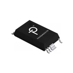
画像は参照用のみです。
STFW3N150
MOSFET N-CH 1500V 2.5A ISOWATT
- メーカー
- Mfr。パート #STFW3N150
- パッケージ TO-3PF
- データシート STFW3N150 DataSheet
- 在庫中4957
100% オリジナル &新しい
出荷の準備ができている24時間
365日の保証
RFQおよびもっと割引を得る
仕様
| Package | Tube |
| Series | PowerMESH™ |
| ProductStatus | Active |
| FETType | N-Channel |
| Technology | MOSFET (Metal Oxide) |
| DraintoSourceVoltage(Vdss) | 1500 V |
| Current-ContinuousDrain(Id)@25°C | 2.5A (Tc) |
| DriveVoltage(MaxRdsOnMinRdsOn) | 10V |
| RdsOn(Max)@IdVgs | 9Ohm @ 1.3A, 10V |
| Vgs(th)(Max)@Id | 5V @ 250µA |
| GateCharge(Qg)(Max)@Vgs | 29.3 nC @ 10 V |
| Vgs(Max) | ±30V |
| InputCapacitance(Ciss)(Max)@Vds | 939 pF @ 25 V |
| PowerDissipation(Max) | 63W (Tc) |
| OperatingTemperature | 150°C (TJ) |
| MountingType | Through Hole |
| SupplierDevicePackage | TO-3PF |
概要
Description
STFW3N150 is likely a specific course or program code, but without more context, it's difficult to provide precise information. Typically, course codes like this are used in educational institutions to categorize subjects or modules within a curriculum. The code might indicate the level of study (e.g., undergraduate or graduate), the subject area (e.g., science, technology), and possibly the number of credits or hours associated with the course.
If you're looking for details about the specific content, prerequisites, or objectives of STFW3N150, I recommend checking the course catalog of the institution offering it or contacting academic advisors. They can provide comprehensive insights into the curriculum, assessment methods, and learning outcomes associated with this course.
If you're looking for details about the specific content, prerequisites, or objectives of STFW3N150, I recommend checking the course catalog of the institution offering it or contacting academic advisors. They can provide comprehensive insights into the curriculum, assessment methods, and learning outcomes associated with this course.
Features
The STFW3N150 is an N-channel MOSFET designed for high-efficiency power applications. Key features include:
1. Voltage Rating: Supports a drain-source voltage (V_DS) of up to 150V, making it suitable for high voltage applications.
2. Current Rating: Capable of handling continuous drain current (I_D) up to 30A, providing robust performance in demanding environments.
3. Low R_DS(on): Offers a low on-resistance, typically around 0.35 Ohms, enhancing efficiency by reducing power losses during operation.
4. Fast Switching Speed: Designed for rapid switching, which is beneficial for applications like DC-DC converters, inverters, and motor control.
5. Thermal Performance: Equipped with a high thermal conductivity package that helps manage heat dissipation effectively.
6. Gate Threshold Voltage: Features a low gate threshold voltage (V_GS(th)), facilitating easier drive requirements.
7. Package Type: Available in various package types, including TO-220 and DPAK, allowing for flexible integration into different circuit designs.
These characteristics make the STFW3N150 suitable for applications in power supplies, automotive systems, and industrial controls.
1. Voltage Rating: Supports a drain-source voltage (V_DS) of up to 150V, making it suitable for high voltage applications.
2. Current Rating: Capable of handling continuous drain current (I_D) up to 30A, providing robust performance in demanding environments.
3. Low R_DS(on): Offers a low on-resistance, typically around 0.35 Ohms, enhancing efficiency by reducing power losses during operation.
4. Fast Switching Speed: Designed for rapid switching, which is beneficial for applications like DC-DC converters, inverters, and motor control.
5. Thermal Performance: Equipped with a high thermal conductivity package that helps manage heat dissipation effectively.
6. Gate Threshold Voltage: Features a low gate threshold voltage (V_GS(th)), facilitating easier drive requirements.
7. Package Type: Available in various package types, including TO-220 and DPAK, allowing for flexible integration into different circuit designs.
These characteristics make the STFW3N150 suitable for applications in power supplies, automotive systems, and industrial controls.
Package
The STFW3N150 is typically packaged in a TO-220 format. This package type is designed for power transistors and provides good thermal performance and ease of mounting on heat sinks.
Pinout
The STFW3N150 is an N-channel MOSFET with a pin count of 3. The pins are typically designated as follows:
1. Gate (G) - This pin is used to control the MOSFET. By applying a voltage to the gate, you can turn the device on or off, allowing current to flow between the drain and source.
2. Drain (D) - This is the pin through which the output current flows when the MOSFET is in the "on" state. The drain is connected to the load.
3. Source (S) - This pin is connected to the ground or the negative side of the circuit. When the MOSFET is on, current flows from the drain to the source.
The STFW3N150 is designed for high-voltage applications, with a maximum drain-source voltage (V_DS) of 150V and a continuous drain current (I_D) rating that allows it to handle substantial loads efficiently.
1. Gate (G) - This pin is used to control the MOSFET. By applying a voltage to the gate, you can turn the device on or off, allowing current to flow between the drain and source.
2. Drain (D) - This is the pin through which the output current flows when the MOSFET is in the "on" state. The drain is connected to the load.
3. Source (S) - This pin is connected to the ground or the negative side of the circuit. When the MOSFET is on, current flows from the drain to the source.
The STFW3N150 is designed for high-voltage applications, with a maximum drain-source voltage (V_DS) of 150V and a continuous drain current (I_D) rating that allows it to handle substantial loads efficiently.
Manufacturer
The STFW3N150 is manufactured by STMicroelectronics, a global semiconductor company. STMicroelectronics specializes in the design, development, and production of a wide range of semiconductor devices and solutions, including power management, microcontrollers, sensors, and analog devices. The company serves various industries such as automotive, industrial, personal electronics, and communications. Founded in 1987, STMicroelectronics is headquartered in Geneva, Switzerland, and operates in numerous countries worldwide, focusing on innovation and sustainability in its product offerings.
Application
The STFW3N150 is a high-voltage N-channel MOSFET primarily used in applications such as power supplies, motor drives, and industrial automation. Its features make it suitable for high-frequency switching, power management in converters, and energy-efficient designs. The device is also utilized in automotive applications and renewable energy systems, including solar inverters, due to its robustness and efficiency in handling high voltages.
Equivalent
The STFW3N150 is a N-channel MOSFET. Equivalent products include:
1. IRF150 - International Rectifier
2. FQP50N150 - Fairchild Semiconductor
3. MTP50N15 - ON Semiconductor
4. BTA50N150 - NXP Semiconductors
Always check datasheets to confirm specifications match your requirements.
1. IRF150 - International Rectifier
2. FQP50N150 - Fairchild Semiconductor
3. MTP50N15 - ON Semiconductor
4. BTA50N150 - NXP Semiconductors
Always check datasheets to confirm specifications match your requirements.
出荷
出荷方法私たち
DHL、FedEx、TNT、UPS、またはあなたの選択の他の運送業者を通じてグローバルな出荷サービスを提供します。
出荷料参照(DHL/FedEx):
DHL の: 配送費は25ドル〜45ドル(0.5kg)の範囲で、推定配送時間は2〜5営業日です。
フェデックス: 配送費は25ドル〜40ドル(0.5kg)の範囲で、推定配送時間は3〜7営業日。
UPS の: 配送費は25ドル〜45ドル(0.5kg)の範囲で、推定配送時間は3〜7営業日。
TNT社: 配送費は25ドル〜65ドル(0.5kg)の範囲で、推定配送時間は3〜7営業日。
EMS: 配送料金は30〜50ドル(0.5kg)の範囲で、推定配送時間は7〜15営業日です。
登録航空郵便: 配送費は2〜4ドル(0.1kg)で、推定配送時間は5〜20営業日です。
支払い
Payment Methods
支払い期間は100%前払いです。
現在、下記の支払い方法のみを受け入れています。:
1. ペイパル
2. クレジット・デビットカード
3. ワイヤー 転送
類似
-
![MX25V1635FZNI]() MX25V1635FZNI
MX25V1635FZNI
Macronix
-
![MX29F400CBTI-70G]() MX29F400CBTI-70G
MX29F400CBTI-70G
Macronix
-
![MX66U1G45GXDI00]() MX66U1G45GXDI00
MX66U1G45GXDI00
Macronix
-
![MX25R3235FZNIL0]() MX25R3235FZNIL0
MX25R3235FZNIL0
Macronix
-
![MX30LF2G28AD-TI]() MX30LF2G28AD-TI
MX30LF2G28AD-TI
Macronix
-
![MX25L8035EM2I-10G]() MX25L8035EM2I-10G
MX25L8035EM2I-10G
Macronix
-
![MX25L6433FM2I-08G]() MX25L6433FM2I-08G
MX25L6433FM2I-08G
Macronix
-
![MX25L12833FZ2I-10G]() MX25L12833FZ2I-10..
MX25L12833FZ2I-10..
Macronix
-
![MX25L12833FZNI-10G]() MX25L12833FZNI-10..
MX25L12833FZNI-10..
Macronix
-
![MX25L25735FMI-10G]() MX25L25735FMI-10G
MX25L25735FMI-10G
Macronix
-
![MX66U1G45GMI00]() MX66U1G45GMI00
MX66U1G45GMI00
Macronix
-
![MX25V8035FM2I]() MX25V8035FM2I
MX25V8035FM2I
Macronix