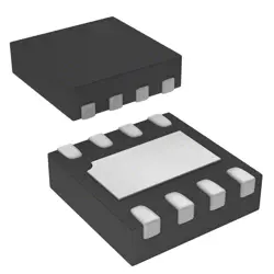
画像は参照用のみです。
SN74LVC1G374DCKR
IC FF D-TYPE SNGL 1BIT SC70-6
- メーカー
- Mfr。パート #SN74LVC1G374DCKR
- パッケージ
- データシート SN74LVC1G374DCKR DataSheet
- 在庫中9041
100% オリジナル &新しい
出荷の準備ができている24時間
365日の保証
RFQおよびもっと割引を得る
仕様
| Supplier | Texas Instruments |
| Package | Tape & Reel (TR),Cut Tape (CT) |
| Series | 74LVC |
| ProductStatus | Active |
| Function | Standard |
| Type | D-Type |
| OutputType | Tri-State |
| NumberofElements | 1 |
| NumberofBitsperElement | 1 |
| ClockFrequency | 175 MHz |
| MaxPropagationDelay@VMaxCL | 4ns @ 5V, 50pF |
| TriggerType | Positive Edge |
| Current-OutputHighLow | 32mA, 32mA |
| Voltage-Supply | 1.65V ~ 5.5V |
| Current-Quiescent(Iq) | 10 µA |
| InputCapacitance | 3 pF |
| OperatingTemperature | -40°C ~ 125°C (TA) |
| MountingType | Surface Mount |
| SupplierDevicePackage | SC-70-6 |
概要
Description
SN74LVC1G374DCKR is an 8-bit, edge-triggered D-type register (flip-flop) with 3-state outputs from TI’s LVC family. It has eight data inputs (D0–D7), eight outputs (Q0–Q7), a clock input (CLK), and an output-enable input (G). On the rising edge of CLK, the data on D0–D7 are captured and appear on Q0–Q7. The G input controls the eight outputs: when enabled, the outputs drive the bus; when disabled, the outputs go high impedance for bus sharing. Operates from a 1.65–3.6 V supply, making it suitable for low-voltage systems and compatible with TTL/CMOS logic levels. The DCKR package is TI’s compact form factor (RoHS-compliant). Typical uses include buffering and storing data on a microcontroller bus, buffering between peripherals, and small-scale data-registering in compact systems. For exact timing, drive requirements, and electrical specs, consult the TI datasheet.
Features
Here are the main features of SN74LVC1G374DCKR:
- 8-bit D-type register with 3-state outputs
- Positive-edge-triggered clock
- Output enable input (G) for tri-state outputs
- Single-supply operation: 1.65 V to 3.6 V (LVC CMOS)
- Low-power CMOS technology with fast switching
- ESD protection; RoHS-compliant packaging (DCKR)
- 8-bit D-type register with 3-state outputs
- Positive-edge-triggered clock
- Output enable input (G) for tri-state outputs
- Single-supply operation: 1.65 V to 3.6 V (LVC CMOS)
- Low-power CMOS technology with fast switching
- ESD protection; RoHS-compliant packaging (DCKR)
Package
DCKR indicates TI’s DCK package with Tape‑and‑Reel. For SN74LVC1G374DCKR, it is a DCK‑20 (20‑pin, TSSOP‑like) package.
Pinout
- Pin count: 20 pins.
- Function: 8-bit D-type edge-triggered register with 3-state outputs. D0–D7 are data inputs; Q0–Q7 are outputs; data is captured on the rising edge of CLK; OE (active-low) enables/disables the outputs; VCC and GND present.
- Function: 8-bit D-type edge-triggered register with 3-state outputs. D0–D7 are data inputs; Q0–Q7 are outputs; data is captured on the rising edge of CLK; OE (active-low) enables/disables the outputs; VCC and GND present.
Manufacturer
- Manufacturer: Texas Instruments (TI)
- Kind of company: American multinational semiconductor company that designs and manufactures analog and digital integrated circuits and other electronic components.
- Kind of company: American multinational semiconductor company that designs and manufactures analog and digital integrated circuits and other electronic components.
Application
- D-type latch/flip-flop for fast data storage and timing control
- 3-state outputs for buffering and sharing data on a common bus
- Pipeline stages and address/data latching in microcontrollers, memory, and DSPs
- Clock-domain crossing and timing synchronization in mixed-voltage systems
- Compact, low-power device suitable for portable, automotive, and consumer electronics use
Equivalent
Equivalent parts (same function in the LVC1G family):
- 74LVC1G374 (Nexperia, formerly NXP)
- 74LVC1G374 (On Semiconductor)
Note: verify exact package/pinout with a cross-reference tool to ensure compatibility with your board.
- 74LVC1G374 (Nexperia, formerly NXP)
- 74LVC1G374 (On Semiconductor)
Note: verify exact package/pinout with a cross-reference tool to ensure compatibility with your board.
出荷
出荷方法私たち
DHL、FedEx、TNT、UPS、またはあなたの選択の他の運送業者を通じてグローバルな出荷サービスを提供します。
出荷料参照(DHL/FedEx):
DHL の: 配送費は25ドル〜45ドル(0.5kg)の範囲で、推定配送時間は2〜5営業日です。
フェデックス: 配送費は25ドル〜40ドル(0.5kg)の範囲で、推定配送時間は3〜7営業日。
UPS の: 配送費は25ドル〜45ドル(0.5kg)の範囲で、推定配送時間は3〜7営業日。
TNT社: 配送費は25ドル〜65ドル(0.5kg)の範囲で、推定配送時間は3〜7営業日。
EMS: 配送料金は30〜50ドル(0.5kg)の範囲で、推定配送時間は7〜15営業日です。
登録航空郵便: 配送費は2〜4ドル(0.1kg)で、推定配送時間は5〜20営業日です。
支払い
Payment Methods
支払い期間は100%前払いです。
現在、下記の支払い方法のみを受け入れています。:
1. ペイパル
2. クレジット・デビットカード
3. ワイヤー 転送
類似
-
![MX25L3233FZBI-08Q]() MX25L3233FZBI-08Q
Macronix
-
![MX25V2033FM1I]() MX25V2033FM1I
Macronix
-
![MX25V16066M2I02]() MX25V16066M2I02
Macronix
-
![MX30LF2G28AD-TI]() MX30LF2G28AD-TI
Macronix
-
![MX25L25673GMI-10G]() MX25L25673GMI-10G
Macronix
-
![MX29GL512FHXFI-11G]() MX29GL512FHXFI-11..
Macronix
-
![MX25U51279GXDR00]() MX25U51279GXDR00
Macronix
-
![MX25L2006EM1I-12G]() MX25L2006EM1I-12G
Macronix
-
![MX25R1635FZUIH0]() MX25R1635FZUIH0
Macronix
-
![MX25L12833FM2I-10G]() MX25L12833FM2I-10..
Macronix
-
![MX25L12833FZ2I-10G]() MX25L12833FZ2I-10..
Macronix
-
![MX25L12833FZNI-10G]() MX25L12833FZNI-10..
Macronix