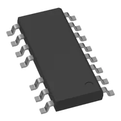
画像は参照用のみです。
SN74HCS574QPWRQ1
AUTOMOTIVE OCTAL EDGE-TRIGGERED
- メーカー
- Mfr。パート #SN74HCS574QPWRQ1
- パッケージ
- データシート SN74HCS574QPWRQ1 DataSheet
- 在庫中7018
100% オリジナル &新しい
出荷の準備ができている24時間
365日の保証
RFQおよびもっと割引を得る
仕様
| Supplier | Texas Instruments |
| Package | Tape & Reel (TR),Cut Tape (CT) |
| ProductStatus | Active |
| Function | Standard |
| Type | D-Type |
| OutputType | Tri-State |
| NumberofElements | 1 |
| NumberofBitsperElement | 8 |
| ClockFrequency | 135 MHz |
| MaxPropagationDelay@VMaxCL | 11ns @ 6V, 50pF |
| TriggerType | Positive Edge |
| Current-OutputHighLow | 7.8mA, 7.8mA |
| Voltage-Supply | 2V ~ 6V |
| Current-Quiescent(Iq) | 2 µA |
| InputCapacitance | 5 pF |
| OperatingTemperature | -40°C ~ 125°C (TA) |
| MountingType | Surface Mount |
| SupplierDevicePackage | 20-TSSOP |
概要
Description
SN74HCS574QPWRQ1 is an 8-bit, edge-triggered D-type register with 3-state outputs from TI’s 74HCS CMOS family. It has eight data inputs (D0–D7), a single clock (CP), and eight tri-state outputs (Q0–Q7) controlled by an active-low output enable (OE). On the rising edge of CP, the D inputs are latched to Q outputs; OE can tri-state all outputs to allow bus sharing when disabled. The device operates from 2.0 to 6.0 V (typical 5 V) with CMOS inputs that are TTL-compatible. It’s commonly used for data storage, bus buffering, and interfacing microprocessors or other digital ICs. The QPWRQ1 suffix indicates TI’s RoHS-compliant packaging variant for this device.
Features
Here are concise features of SN74HCS574QPWRQ1:
- 8-bit, edge-triggered D-type register (D0–D7) with Q0–Q7 outputs
- Rising-edge clock (CLK) captures data
- 3-state outputs with Output Enable (OE\) input; outputs go High-Z when OE\ is high
- TTL-compatible inputs; High-speed CMOS (HCS) device
- Vcc typically 4.5V–5.5V (5V nominal)
- Low static/dynamic power consumption
- Suitable for bus interfacing and data buffering
- 20-pin plastic package, RoHS-compliant (QPWRQ1)
- Nondestructive reads; data retained until next clock edge
Applications: microprocessor/data buses, latch/register buffering, and parallel data conversion interfaces.
Package
20-pin Plastic Small-Outline (SOIC) package, RoHS-compliant (Q1 tape-and-reel available).
Pinout
- Pin count: 20 pins (DIP20/SOIC-20/TSSOP-20 variants in the SN74HCS574QPWRQ1 family).
- Function: 8-bit D-type edge-triggered register with 3-state outputs. It samples D0–D7 on the rising edge of CLK and presents the data on Q0–Q7; outputs are enabled/disabled by the active-low Output Enable (OE) input (high → tri-state; low → valid outputs).
- Function: 8-bit D-type edge-triggered register with 3-state outputs. It samples D0–D7 on the rising edge of CLK and presents the data on Q0–Q7; outputs are enabled/disabled by the active-low Output Enable (OE) input (high → tri-state; low → valid outputs).
Manufacturer
- Manufacturer: Texas Instruments (TI)
- What kind of company: A multinational American semiconductor design and manufacturing company that specializes in analog, mixed-signal, and embedded processing ICs and related semiconductor products for a wide range of industries.
- What kind of company: A multinational American semiconductor design and manufacturing company that specializes in analog, mixed-signal, and embedded processing ICs and related semiconductor products for a wide range of industries.
Application
Application areas: Bus interface and buffering for microprocessors/microcontrollers; address latch for multiplexed buses (e.g., 8086); data storage and buffering for peripherals; tri-state bus driver/isolator in memory-mapped I/O; pipeline/register-file style data-path buffering.
Equivalent
Equivalent parts (octal D-type register with 3-state outputs) include TI variants: SN74HC574, SN74HCT574, SN74HCP574, SN74HCS574, SN74LVC574. Other vendors offer 74HC574, 74HCT574, 74LVC574. Note pinout, supply voltage, and I/O thresholds may differ; verify datasheets and cross-reference before substitution.
出荷
出荷方法私たち
DHL、FedEx、TNT、UPS、またはあなたの選択の他の運送業者を通じてグローバルな出荷サービスを提供します。
出荷料参照(DHL/FedEx):
DHL の: 配送費は25ドル〜45ドル(0.5kg)の範囲で、推定配送時間は2〜5営業日です。
フェデックス: 配送費は25ドル〜40ドル(0.5kg)の範囲で、推定配送時間は3〜7営業日。
UPS の: 配送費は25ドル〜45ドル(0.5kg)の範囲で、推定配送時間は3〜7営業日。
TNT社: 配送費は25ドル〜65ドル(0.5kg)の範囲で、推定配送時間は3〜7営業日。
EMS: 配送料金は30〜50ドル(0.5kg)の範囲で、推定配送時間は7〜15営業日です。
登録航空郵便: 配送費は2〜4ドル(0.1kg)で、推定配送時間は5〜20営業日です。
支払い
Payment Methods
支払い期間は100%前払いです。
現在、下記の支払い方法のみを受け入れています。:
1. ペイパル
2. クレジット・デビットカード
3. ワイヤー 転送
類似
-
![MX29F400CBTI-70G]() MX29F400CBTI-70G
Macronix
-
![MX30LF2G28AD-TI]() MX30LF2G28AD-TI
Macronix
-
![MX25L25673GMI-08G]() MX25L25673GMI-08G
Macronix
-
![MX29GL512FHXFI-11G]() MX29GL512FHXFI-11..
Macronix
-
![MX25U51279GXDR00]() MX25U51279GXDR00
Macronix
-
![MX25R1635FZUIH0]() MX25R1635FZUIH0
Macronix
-
![MX25V1635FM2I]() MX25V1635FM2I
Macronix
-
![MX25L12833FZ2I-10G]() MX25L12833FZ2I-10..
Macronix
-
![MX25L12835FZ2I-10G]() MX25L12835FZ2I-10..
Macronix
-
![MX29LV640ETTI-70G]() MX29LV640ETTI-70G
Macronix
-
![MX25L25735FMI-10G]() MX25L25735FMI-10G
Macronix
-
![MX25L4006EM2I-12G]() MX25L4006EM2I-12G
Macronix