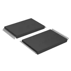
画像は参照用のみです。
SM41J256M16M
- メーカー
- Mfr。パート #SM41J256M16M
- パッケージ
- データシート
- 在庫中18537
100% オリジナル &新しい
出荷の準備ができている24時間
365日の保証
RFQおよびもっと割引を得る
仕様
| Manufacturer | JLCPCB Assembly |
| Package | BGA96_13.5X9mm |
概要
Description
The SM41J256M16M is a high-performance Dynamic Random Access Memory (DRAM) device, specifically a DDR3 SDRAM, designed for various computing applications. It features a 256M x 16-bit architecture, providing a total capacity of 512 megabits. This memory chip operates at various standard frequencies, typically around 800 MHz, ensuring efficient data transfer rates suitable for modern computing needs.
Key features include a low-voltage operation (usually around 1.5V), enhanced speed, and energy efficiency, making it ideal for use in laptops, desktops, and embedded systems. The SM41J256M16M is designed with advanced memory management capabilities, such as burst mode access and deep sleep functionalities, which contribute to improved performance and reduced power consumption.
Its compatibility with various memory controllers and systems ensures widespread applicability in consumer electronics, telecommunications, and industrial applications. Overall, the SM41J256M16M represents a reliable and efficient solution for meeting the demands of contemporary electronic devices.
Features
The SM41J256M16M is a high-performance DDR3 SDRAM (Dynamic Random Access Memory) chip. Key features include:
1. Capacity: 256 Megabits (32 Megabytes) per chip.
2. Organization: 16 Meg x 16 bits, suitable for various applications.
3. Speed: Supports data rates up to 1866 MT/s, enabling efficient data transfer.
4. Operating Voltage: Typically operates at 1.5V (±0.1V), ensuring energy efficiency.
5. Data Bus: 16-bit wide data bus enhances data transfer capabilities.
6. Latency: Low latency performance, improving response times for applications.
7. Packaging: Available in various package types for flexible integration.
8. Applications: Commonly used in consumer electronics, networking devices, and industrial applications.
This chip is ideal for devices requiring reliable performance and energy efficiency in memory storage.
Package
The SM41J256M16M is typically packaged in a FBGA (Fine Ball Grid Array) format, which allows for a compact design and efficient thermal management.
Pinout
The SM41J256M16M is a 256 Mb (32 MB) NAND Flash memory device with a pin count of 48. It typically uses a TSOP (Thin Small Outline Package) or similar package format.
The primary functions of the SM41J256M16M include:
1. Data Storage: Provides non-volatile storage for various applications, such as smartphones, tablets, and embedded systems.
2. Read/Write Operations: Supports multiple read and write operations, enabling efficient data management.
3. Page and Block Management: Utilizes page and block architectures for data organization, allowing for efficient wear leveling and error management.
4. Interface: Generally operates through a parallel interface for direct communication with a host controller.
For specific applications and performance characteristics, it would be advisable to consult the manufacturer's datasheet.
Manufacturer
The SM41J256M16M is manufactured by Samsung Electronics, a South Korean multinational conglomerate. Samsung is primarily known for its electronics division, which produces a wide range of products, including semiconductors, smartphones, televisions, and home appliances. The company is a leading player in the semiconductor industry, particularly in the production of memory chips like DRAM and NAND flash. Samsung Electronics is part of the larger Samsung Group, which has diversified interests in various sectors, including shipbuilding, construction, and financial services. Overall, Samsung is recognized for its innovation, technological advancements, and significant contributions to the global electronics market.
Application
The SM41J256M16M is a 256 Mb (32 MB) DDR3 SDRAM memory chip commonly used in applications such as smartphones, tablets, digital cameras, automotive electronics, and other consumer electronics. It supports high-speed data processing, making it suitable for gaming devices, networking equipment, and industrial applications where efficient memory access is critical.
Equivalent
The SM41J256M16M chip, a 256Mb DRAM, is equivalent to products like the Micron MT41J256M16HA-15E, Samsung K4B256M16HA, and Hynix H5TQ2G83AFR. Always verify specifications such as speed, voltage, and package type to ensure compatibility when selecting equivalent products.
出荷
出荷方法私たち
DHL、FedEx、TNT、UPS、またはあなたの選択の他の運送業者を通じてグローバルな出荷サービスを提供します。
出荷料参照(DHL/FedEx):
DHL の: 配送費は25ドル〜45ドル(0.5kg)の範囲で、推定配送時間は2〜5営業日です。
フェデックス: 配送費は25ドル〜40ドル(0.5kg)の範囲で、推定配送時間は3〜7営業日。
UPS の: 配送費は25ドル〜45ドル(0.5kg)の範囲で、推定配送時間は3〜7営業日。
TNT社: 配送費は25ドル〜65ドル(0.5kg)の範囲で、推定配送時間は3〜7営業日。
EMS: 配送料金は30〜50ドル(0.5kg)の範囲で、推定配送時間は7〜15営業日です。
登録航空郵便: 配送費は2〜4ドル(0.1kg)で、推定配送時間は5〜20営業日です。
支払い
Payment Methods
支払い期間は100%前払いです。
現在、下記の支払い方法のみを受け入れています。:
1. ペイパル
2. クレジット・デビットカード
3. ワイヤー 転送
類似
-
![MX25R8035FM1IL0]() MX25R8035FM1IL0
Macronix
-
![MX25R3235FZNIL0]() MX25R3235FZNIL0
Macronix
-
![MX25U51279GXDR00]() MX25U51279GXDR00
Macronix
-
![MX25V1635FM2I]() MX25V1635FM2I
Macronix
-
![MX25L12835FZ2I-10G]() MX25L12835FZ2I-10..
Macronix
-
![MX29F040CQI-70G]() MX29F040CQI-70G
Macronix
-
![MX29F040CTI-70G]() MX29F040CTI-70G
Macronix
-
![MX29F800CBTI-70G]() MX29F800CBTI-70G
Macronix
-
![MX29LV640ETTI-70G]() MX29LV640ETTI-70G
Macronix
-
![MX25U51245GZ4I00]() MX25U51245GZ4I00
Macronix
-
![MX66U1G45GMI00]() MX66U1G45GMI00
Macronix
-
![MX29LV040CQI-70G]() MX29LV040CQI-70G
Macronix