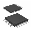
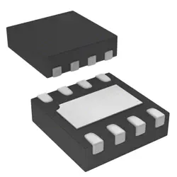
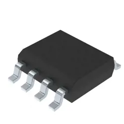
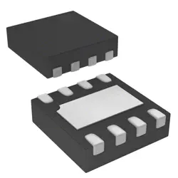
画像は参照用のみです。
RT9624CGQWA
IC GATE DRVR HI/LOW SIDE 8WDFN
- メーカー
- Mfr。パート #RT9624CGQWA
- パッケージ
- データシート
- 在庫中2673
100% オリジナル &新しい
出荷の準備ができている24時間
365日の保証
RFQおよびもっと割引を得る
仕様
| Part Status | Active |
| DigiKey Programmable | Not Verified |
| Driven Configuration | High-Side or Low-Side |
| Channel Type | Synchronous |
| Number of Drivers | 2 |
| Gate Type | MOSFET (N-Channel) |
| Voltage - Supply | 4.5V ~ 13.2V |
| Input Type | Non-Inverting |
| Rise / Fall Time (Typ) | 25ns, 12ns |
| Operating Temperature | -40°C ~ 85°C (TA) |
| Mounting Type | Surface Mount |
| Package / Case | 8-WFDFN Exposed Pad |
| Supplier Device Package | 8-WDFN-SL (2x2) |
| Base Product Number | RT9624 |
| High Side Voltage - Max (Bootstrap) | 46 V |
概要
Description
The RT9624CGQWA is a dual gate driver IC designed for synchronous buck converters, commonly used in computing and consumer electronics. Manufactured by Richtek Technology, this component efficiently drives both high-side and low-side N-MOSFETs, crucial for voltage regulation in modern electronic circuits. It features adaptive dead-time control, which helps prevent shoot-through conditions by ensuring that the high-side and low-side MOSFETs are not on simultaneously. This enhances efficiency and reliability in power management applications.
The RT9624CGQWA operates with a supply voltage range typically between 4.5V to 13.2V, making it versatile for various applications. It usually offers features like undervoltage lockout (UVLO) to protect the system during low power conditions, and it has a fast switching capability to support high-frequency operations. The IC is housed in a thermally efficient and compact package, such as a WDFN package, facilitating heat dissipation and easy integration into PCB designs.
Overall, the RT9624CGQWA is valued for its high performance in regulating power efficiently and is a critical component in systems requiring reliable power conversion.
The RT9624CGQWA operates with a supply voltage range typically between 4.5V to 13.2V, making it versatile for various applications. It usually offers features like undervoltage lockout (UVLO) to protect the system during low power conditions, and it has a fast switching capability to support high-frequency operations. The IC is housed in a thermally efficient and compact package, such as a WDFN package, facilitating heat dissipation and easy integration into PCB designs.
Overall, the RT9624CGQWA is valued for its high performance in regulating power efficiently and is a critical component in systems requiring reliable power conversion.
Features
The RT9624CGQWA is a PWM driver designed for high-performance synchronous rectified buck converters. Key features include:
1. Dual-Channel Design: Supports two high-side and two low-side MOSFETs, enhancing efficiency and power delivery.
2. High-Speed Operation: Optimized for high-frequency applications, contributing to improved transient response and reduced output ripple.
3. Adaptive Dead-Time Control: Minimizes switching losses by adjusting the non-overlapping time between high-side and low-side MOSFETs.
4. Integrated Bootstrap Diode: Simplifies circuit design and reduces component count by incorporating a diode for high-side driver supply.
5. Under-Voltage Lockout (UVLO): Protects the system by disabling the driver outputs when the input voltage is too low.
6. Thermal Protection: Prevents device damage by shutting down the driver when the temperature exceeds a safe threshold.
7. Compact Package: Typically offered in a compact package suitable for space-constrained applications.
These features make the RT9624CGQWA suitable for applications requiring efficient, high-performance power conversion, such as in computing and telecom environments.
1. Dual-Channel Design: Supports two high-side and two low-side MOSFETs, enhancing efficiency and power delivery.
2. High-Speed Operation: Optimized for high-frequency applications, contributing to improved transient response and reduced output ripple.
3. Adaptive Dead-Time Control: Minimizes switching losses by adjusting the non-overlapping time between high-side and low-side MOSFETs.
4. Integrated Bootstrap Diode: Simplifies circuit design and reduces component count by incorporating a diode for high-side driver supply.
5. Under-Voltage Lockout (UVLO): Protects the system by disabling the driver outputs when the input voltage is too low.
6. Thermal Protection: Prevents device damage by shutting down the driver when the temperature exceeds a safe threshold.
7. Compact Package: Typically offered in a compact package suitable for space-constrained applications.
These features make the RT9624CGQWA suitable for applications requiring efficient, high-performance power conversion, such as in computing and telecom environments.
Package
The RT9624CGQWA typically comes in a QFN (Quad Flat No-leads) package, which is compact and suitable for surface-mount technology. This package type is designed for efficient heat dissipation and minimal electrical resistance, making it ideal for high-performance applications.
Pinout
The RT9624CGQWA is a dual MOSFET driver IC designed to drive low-side and high-side N-channel MOSFETs in a synchronous buck converter topology. It typically comes in a 10-pin package, often a WDFN-10L 3x3 package. The primary function of the RT9624CGQWA is to provide adaptive dead-time control, ensuring that both the high-side and low-side MOSFETs are never on at the same time, thus preventing shoot-through currents. The IC also features a built-in internal bootstrap diode for high-side MOSFET driving, and it is optimized for high-frequency applications, enhancing efficiency.
Key pins include:
1. VCC - Supply voltage for the driver.
2. BOOT - Bootstrap capacitor connection.
3. UGATE - High-side MOSFET gate drive output.
4. PHASE - Connection to the high-side MOSFET source and the low-side MOSFET drain.
5. LGATE - Low-side MOSFET gate drive output.
6. GND - Ground connection.
7. PWM - PWM input signal.
8. EN - Enable pin, controlling the operation of the IC.
This dual-driver configuration is commonly used in power management applications for optimizing the performance of power converters.
Key pins include:
1. VCC - Supply voltage for the driver.
2. BOOT - Bootstrap capacitor connection.
3. UGATE - High-side MOSFET gate drive output.
4. PHASE - Connection to the high-side MOSFET source and the low-side MOSFET drain.
5. LGATE - Low-side MOSFET gate drive output.
6. GND - Ground connection.
7. PWM - PWM input signal.
8. EN - Enable pin, controlling the operation of the IC.
This dual-driver configuration is commonly used in power management applications for optimizing the performance of power converters.
Manufacturer
The RT9624CGQWA is manufactured by Richtek Technology Corporation. Richtek is a company that specializes in the design and development of analog integrated circuits, particularly focusing on power management solutions. They provide a wide range of products including voltage regulators, battery management systems, LED drivers, and other power-related components. Richtek is known for its innovation in providing energy-efficient and cost-effective solutions, primarily serving markets in consumer electronics, computing, industrial, and automotive applications.
Application
The RT9624CGQWA is primarily used in voltage regulation applications, particularly in synchronous buck converters. It is suitable for use in high-performance desktop computers, servers, and graphic cards. The component is typically employed to provide efficient power management for microprocessors, memory modules, and other digital ICs, ensuring stable and reliable power delivery in computing and networking systems.
Equivalent
The RT9624CGQWA is a dual MOSFET driver commonly used for synchronous buck applications. Equivalent products from other manufacturers might include the LTC1693 series from Analog Devices, the ISL6620 from Renesas, and the FAN3224 from ON Semiconductor. When selecting an equivalent, ensure compatibility in terms of voltage, current capabilities, and switching speed. Checking data sheets for pin compatibility is also essential.
出荷
出荷方法私たち
DHL、FedEx、TNT、UPS、またはあなたの選択の他の運送業者を通じてグローバルな出荷サービスを提供します。
出荷料参照(DHL/FedEx):
DHL の: 配送費は25ドル〜45ドル(0.5kg)の範囲で、推定配送時間は2〜5営業日です。
フェデックス: 配送費は25ドル〜40ドル(0.5kg)の範囲で、推定配送時間は3〜7営業日。
UPS の: 配送費は25ドル〜45ドル(0.5kg)の範囲で、推定配送時間は3〜7営業日。
TNT社: 配送費は25ドル〜65ドル(0.5kg)の範囲で、推定配送時間は3〜7営業日。
EMS: 配送料金は30〜50ドル(0.5kg)の範囲で、推定配送時間は7〜15営業日です。
登録航空郵便: 配送費は2〜4ドル(0.1kg)で、推定配送時間は5〜20営業日です。
支払い
Payment Methods
支払い期間は100%前払いです。
現在、下記の支払い方法のみを受け入れています。:
1. ペイパル
2. クレジット・デビットカード
3. ワイヤー 転送
類似
-
![MX25L3233FZBI-08Q]() MX25L3233FZBI-08Q
Macronix
-
![MX25V1635FZNI]() MX25V1635FZNI
Macronix
-
![MX25V4035FZUI]() MX25V4035FZUI
Macronix
-
![MX30LF2G28AD-TI]() MX30LF2G28AD-TI
Macronix
-
![MX25L25673GMI-08G]() MX25L25673GMI-08G
Macronix
-
![MX25L25673GMI-10G]() MX25L25673GMI-10G
Macronix
-
![MX25U51279GXDR00]() MX25U51279GXDR00
Macronix
-
![MX25U25643GZNI00]() MX25U25643GZNI00
Macronix
-
![MX25R1635FZUIH0]() MX25R1635FZUIH0
Macronix
-
![MX25V1635FM2I]() MX25V1635FM2I
Macronix
-
![MX25U3232FZBI02]() MX25U3232FZBI02
Macronix
-
![MX25L12833FM2I-10G]() MX25L12833FM2I-10..
Macronix