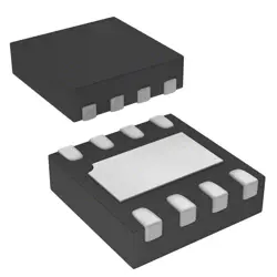
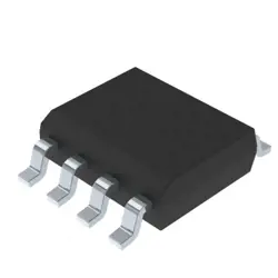
画像は参照用のみです。
QPQ1285TR7
Signal Conditioning Band 41 BW 194MHz LowDrift BAW
- メーカー
- Mfr。パート #QPQ1285TR7
- パッケージ
- データシート QPQ1285TR7 DataSheet
- 在庫中3247
100% オリジナル &新しい
出荷の準備ができている24時間
365日の保証
RFQおよびもっと割引を得る
仕様
| Packaging | MouseReel |
| Standard Pack Qty | 2500 |
概要
Description
QPQ1285TR7 is a specific part number that generally refers to an integrated circuit or semiconductor component, typically used in various electronic applications. While the exact specifications can vary, components like this are often found in consumer electronics, automotive systems, or industrial applications.
Key features may include its operational voltage, current ratings, package type, and suitability for specific applications such as signal processing, power management, or communication systems. The "TR7" designation often indicates the packaging or reel size for assembly processes, while “QPQ1285” may denote the specific functionality or technology utilized in the chip.
To obtain accurate technical details, including datasheets, pin configurations, and application circuits, one should consult the manufacturer's documentation or relevant electronics databases.
Features
The QPQ1285TR7 is a high-performance N-channel MOSFET designed for power management applications. Key features include:
1. Voltage Rating: It typically supports a maximum drain-source voltage (V_DS) of around 30V, making it suitable for low-to-moderate voltage applications.
2. Current Handling: The device can handle continuous drain currents (I_D) up to approximately 30A, providing robust performance for various electrical loads.
3. Low R_DS(on): It features a low on-resistance (R_DS(on)), typically around 10-15 mΩ, which reduces power losses and improves efficiency in switching applications.
4. Fast Switching Speed: Designed for quick turn-on and turn-off, it enhances switching efficiency, beneficial for high-frequency applications.
5. Thermal Management: The package design supports effective heat dissipation, allowing for reliable operation under heavy load conditions.
6. Applications: Commonly used in switching power supplies, motor control, and DC-DC converters.
These features make the QPQ1285TR7 an ideal choice for various consumer electronics and industrial applications.
Package
The QPQ1285TR7 is packaged in a 128-pin TQFP (Thin Quad Flat Package). This type of package is designed for surface mounting and features a thin profile with pins around the edges for easy integration into electronic circuits.
Pinout
The QPQ1285TR7 is a high-performance dual-channel operational amplifier with a pin count of 8. It typically features a variety of functions, including:
1. Input Pins (In+ and In-): For differential signal input.
2. Output Pins (Out): For the amplified output signal.
3. Power Supply Pins (V+ and V-): For connecting to the positive and negative supply voltages, respectively.
4. Common Mode Voltage Pin (CMV): For setting the common mode voltage level.
5. Compensation Pin: For frequency compensation and stability.
The QPQ1285TR7 is designed for applications requiring high accuracy, low noise, and low distortion, making it suitable for precision signal processing. Please refer to the specific datasheet for detailed electrical characteristics and application guidelines.
Manufacturer
The QPQ1285TR7 is manufactured by Qorvo, Inc., a prominent semiconductor company based in the United States. Qorvo specializes in designing and supplying radio frequency (RF) solutions, including devices used in various applications like mobile devices, wireless communication, and IoT (Internet of Things) technologies. The company focuses on enabling connectivity in a wide range of electronic products, utilizing advanced technology to enhance performance and efficiency. Qorvo serves customers in diverse sectors, including automotive, aerospace, and consumer electronics, positioning itself as a key player in the semiconductor industry.
Application
The QPQ1285TR7 is a high-performance, low-dropout (LDO) voltage regulator commonly used in applications requiring stable power supply, such as consumer electronics, automotive systems, and telecommunications equipment. It is ideal for powering microcontrollers, sensors, and RF components in portable devices, as well as in battery-operated applications where efficiency is crucial.
出荷
出荷方法私たち
DHL、FedEx、TNT、UPS、またはあなたの選択の他の運送業者を通じてグローバルな出荷サービスを提供します。
出荷料参照(DHL/FedEx):
DHL の: 配送費は25ドル〜45ドル(0.5kg)の範囲で、推定配送時間は2〜5営業日です。
フェデックス: 配送費は25ドル〜40ドル(0.5kg)の範囲で、推定配送時間は3〜7営業日。
UPS の: 配送費は25ドル〜45ドル(0.5kg)の範囲で、推定配送時間は3〜7営業日。
TNT社: 配送費は25ドル〜65ドル(0.5kg)の範囲で、推定配送時間は3〜7営業日。
EMS: 配送料金は30〜50ドル(0.5kg)の範囲で、推定配送時間は7〜15営業日です。
登録航空郵便: 配送費は2〜4ドル(0.1kg)で、推定配送時間は5〜20営業日です。
支払い
Payment Methods
支払い期間は100%前払いです。
現在、下記の支払い方法のみを受け入れています。:
1. ペイパル
2. クレジット・デビットカード
3. ワイヤー 転送
類似
-
![MX25R8035FM1IL0]() MX25R8035FM1IL0
Macronix
-
![MX25L3233FM1I-08Q]() MX25L3233FM1I-08Q
Macronix
-
![MX25V1635FZNI]() MX25V1635FZNI
Macronix
-
![MX25V1635FZNQ03]() MX25V1635FZNQ03
Macronix
-
![MX66U1G45GXDI00]() MX66U1G45GXDI00
Macronix
-
![MX25V2033FM1I]() MX25V2033FM1I
Macronix
-
![MX25V16066M1I02]() MX25V16066M1I02
Macronix
-
![MX25L25673GMI-08G]() MX25L25673GMI-08G
Macronix
-
![MX25L2006EM1I-12G]() MX25L2006EM1I-12G
Macronix
-
![MX25R1635FZUIH0]() MX25R1635FZUIH0
Macronix
-
![MX25V1635FM2I]() MX25V1635FM2I
Macronix
-
![MX25U6435FM2I-10G]() MX25U6435FM2I-10G
Macronix