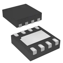
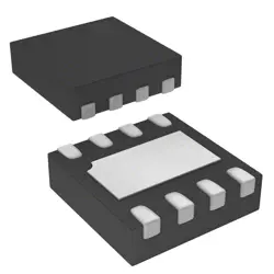
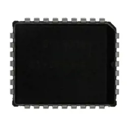
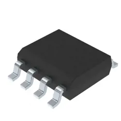
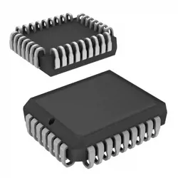
画像は参照用のみです。
PI6C20400BLEX
IC CLOCK BUFFER 1:4 28TSSOP
- メーカー
- Mfr。パート #PI6C20400BLEX
- パッケージ TSSOP-28
- データシート PI6C20400BLEX DataSheet
- 在庫中2669
100% オリジナル &新しい
出荷の準備ができている24時間
365日の保証
RFQおよびもっと割引を得る
仕様
| Package | Tape & Reel (TR),Cut Tape (CT) |
| ProductStatus | Active |
| PLL | Yes |
| MainPurpose | PCI Express (PCIe) |
| Input | HCSL |
| Output | HCSL |
| NumberofCircuits | 1 |
| Ratio-Input:Output | 1:4 |
| Differential-Input:Output | Yes/Yes |
| Frequency-Max | 400MHz |
| Voltage-Supply | 3.135V ~ 3.465V |
| OperatingTemperature | -40°C ~ 85°C |
| MountingType | Surface Mount |
| Package/Case | 28-TSSOP (0.173, 4.40mm Width) |
概要
Description
The PI6C20400BLEX is a high-performance clock buffer designed for various applications, including telecommunications, data centers, and computing systems. It features multiple output drivers that can distribute a single clock signal to multiple devices with minimal skew and jitter. The device typically offers low propagation delay, high output drive strength, and supports a wide voltage range, making it suitable for interfacing with different logic families.
With its robust architecture, the PI6C20400BLEX ensures signal integrity and reliability in demanding environments, helping to enhance the overall performance of electronic systems. Additionally, it often incorporates features such as power-saving modes and programmable settings to optimize power consumption according to the specific needs of the application.
Overall, the PI6C20400BLEX serves as a reliable solution for clock distribution in modern electronic designs, contributing to improved efficiency and performance in high-speed data operations.
Features
The PI6C20400BLEX is a versatile, low-power clock buffer and fanout device designed for high-performance applications. Key features include:
1. Fanout Capability: Supports up to 4 outputs with a high fanout ratio, ideal for distributing clock signals across multiple components.
2. Low Skew: Provides minimal skew between outputs, ensuring synchronized signal delivery critical for timing-sensitive applications.
3. Wide Voltage Range: Operates within a voltage range of 1.2V to 3.6V, making it compatible with various digital systems.
4. Low Power Consumption: Designed for efficiency, it minimizes power usage, which is essential for battery-powered devices.
5. High Frequency Support: Capable of handling clock frequencies up to 200 MHz, suitable for high-speed data applications.
6. Single-Ended and Differential Inputs: Supports both types of input signals, enhancing flexibility in design.
7. Thermal and ESD Protection: Includes features that offer enhanced robustness against thermal and electrostatic discharge damage.
These features make the PI6C20400BLEX suitable for applications in telecommunications, data centers, and consumer electronics.
Package
The PI6C20400BLEX is available in a 32-pin QFN (Quad Flat No-lead) package type.
Pinout
The PI6C20400BLEX is a PCIe switch with a pin count of 64. It operates as a multi-port switch to manage data traffic between multiple PCIe devices. The main functions of the PI6C20400BLEX include facilitating data transfer between devices, providing isolation between different PCIe endpoints, and enabling dynamic bandwidth allocation. It supports various configurations such as single and dual-port setups and can extend PCIe connectivity, making it suitable for applications in servers, storage systems, and high-performance computing. The device is designed with power efficiency and performance scalability in mind.
Manufacturer
The PI6C20400BLEX is manufactured by Parallax Semiconductor, Inc. Parallax is a technology company that specializes in developing high-performance, low-latency integrated circuits (ICs) and semiconductor solutions. They focus on providing advanced products for various applications, including high-speed data communications, networking, and consumer electronics. The company is known for its innovation in chip design and is positioned within the broader semiconductor industry, which encompasses companies that design and manufacture electronic components used in a wide range of devices. Parallax Semiconductor aims to deliver cutting-edge technology that supports the growing demand for efficient and reliable electronic systems.
Application
The PI6C20400BLEX is a high-performance clock buffer and fanout device commonly used in applications such as telecommunications, data centers, and high-speed computing. It provides signal integrity improvement and minimizes clock skew in systems requiring multiple clock outputs from a single source. Typical areas of application include network switches, routers, server motherboards, and high-frequency test equipment.
Equivalent
The PI6C20400BLEX chip is a PCIe clock generator. Equivalent products include:
1. IDT/OSPI 8P49V5901
2. IDT 8T49N001
3. SiTime SiT8008
4. Texas Instruments CDCE62005
Ensure to check specific datasheets for detailed compatibility and feature comparisons.
1. IDT/OSPI 8P49V5901
2. IDT 8T49N001
3. SiTime SiT8008
4. Texas Instruments CDCE62005
Ensure to check specific datasheets for detailed compatibility and feature comparisons.
出荷
出荷方法私たち
DHL、FedEx、TNT、UPS、またはあなたの選択の他の運送業者を通じてグローバルな出荷サービスを提供します。
出荷料参照(DHL/FedEx):
DHL の: 配送費は25ドル〜45ドル(0.5kg)の範囲で、推定配送時間は2〜5営業日です。
フェデックス: 配送費は25ドル〜40ドル(0.5kg)の範囲で、推定配送時間は3〜7営業日。
UPS の: 配送費は25ドル〜45ドル(0.5kg)の範囲で、推定配送時間は3〜7営業日。
TNT社: 配送費は25ドル〜65ドル(0.5kg)の範囲で、推定配送時間は3〜7営業日。
EMS: 配送料金は30〜50ドル(0.5kg)の範囲で、推定配送時間は7〜15営業日です。
登録航空郵便: 配送費は2〜4ドル(0.1kg)で、推定配送時間は5〜20営業日です。
支払い
Payment Methods
支払い期間は100%前払いです。
現在、下記の支払い方法のみを受け入れています。:
1. ペイパル
2. クレジット・デビットカード
3. ワイヤー 転送
類似
-
![MX25L3233FM1I-08Q]() MX25L3233FM1I-08Q
Macronix
-
![MX25V5126FM1I]() MX25V5126FM1I
Macronix
-
![MX30LF2G28AD-TI]() MX30LF2G28AD-TI
Macronix
-
![MX25R1635FZUIH0]() MX25R1635FZUIH0
Macronix
-
![MX25U3232FZBI02]() MX25U3232FZBI02
Macronix
-
![MX29F040CQI-70G]() MX29F040CQI-70G
Macronix
-
![MX25U51245GZ4I00]() MX25U51245GZ4I00
Macronix
-
![MX25L1006EMI-10G]() MX25L1006EMI-10G
Macronix
-
![MX25L4006EM2I-12G]() MX25L4006EM2I-12G
Macronix
-
![MX25V8035FM2I]() MX25V8035FM2I
Macronix
-
![MX25L12872FM2I-10G]() MX25L12872FM2I-10..
Macronix
-
![MX29LV040CQI-70G]() MX29LV040CQI-70G
Macronix