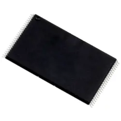
画像は参照用のみです。
PCA9306FMUTCG
IC TRNSLTR BIDIRECTIONAL 8UDFN
- メーカー
- Mfr。パート #PCA9306FMUTCG
- パッケージ 8-UFDFN
- データシート
- 在庫中4747
100% オリジナル &新しい
出荷の準備ができている24時間
365日の保証
RFQおよびもっと割引を得る
仕様
| Package | Tape & Reel (TR),Cut Tape (CT) |
| ProductStatus | Active |
| TranslatorType | Voltage Level |
| ChannelType | Bidirectional |
| NumberofCircuits | 1 |
| ChannelsperCircuit | 2 |
| Voltage-VCCA | 1 V ~ 3.6 V |
| Voltage-VCCB | 1.8 V ~ 5.5 V |
| OutputType | Open Drain |
| OperatingTemperature | -55°C ~ 125°C (TA) |
| Features | Auto-Direction Sensing |
| MountingType | Surface Mount |
| Package/Case | 8-UFDFN |
概要
Description
The PCA9306FMUTCG is a dual bidirectional I²C bus level shifter designed by NXP Semiconductors. It facilitates communication between devices operating at different voltage levels, typically between 1.2V and 5.5V. The device allows for seamless data transfer on I²C buses by translating the signals from one voltage level to another, ensuring compatibility between components like microcontrollers and sensors that may operate at different power levels.
Key features include low propagation delay, high-speed operation up to 1 MHz, and the ability to handle multiple I²C devices on each side. The PCA9306 is particularly useful in applications that require interfacing legacy components with modern systems or integrating components with varying power supply requirements. Its compact package and ease of integration make it ideal for use in consumer electronics, industrial controls, and automotive applications.
Key features include low propagation delay, high-speed operation up to 1 MHz, and the ability to handle multiple I²C devices on each side. The PCA9306 is particularly useful in applications that require interfacing legacy components with modern systems or integrating components with varying power supply requirements. Its compact package and ease of integration make it ideal for use in consumer electronics, industrial controls, and automotive applications.
Features
The PCA9306FMUTCG is a dual bidirectional I2C bus buffer designed to enable I2C communication between devices operating at different voltage levels. Key features include:
1. Dual Supply Voltage: Supports different voltage levels on each side (0.8V to 5.5V), allowing interfacing between low-voltage and higher-voltage I2C devices.
2. Bidirectional Buffering: Facilitates bidirectional data transmission, ensuring signal integrity in both directions.
3. Open-Drain Output: Compatible with open-drain I2C devices, allowing for multiple devices to share the bus without conflicts.
4. Low Propagation Delay: Ensures minimal delay in signal transmission, enhancing communication speed.
5. High Speed: Supports standard I2C speeds of up to 1 MHz.
6. Low Power Consumption: Designed for energy efficiency, making it suitable for battery-operated devices.
7. Robust Design: Features built-in ESD protection (up to ±8kV) to enhance reliability.
This makes the PCA9306FMUTCG ideal for applications where voltage level shifting is necessary, such as in mixed-voltage systems.
1. Dual Supply Voltage: Supports different voltage levels on each side (0.8V to 5.5V), allowing interfacing between low-voltage and higher-voltage I2C devices.
2. Bidirectional Buffering: Facilitates bidirectional data transmission, ensuring signal integrity in both directions.
3. Open-Drain Output: Compatible with open-drain I2C devices, allowing for multiple devices to share the bus without conflicts.
4. Low Propagation Delay: Ensures minimal delay in signal transmission, enhancing communication speed.
5. High Speed: Supports standard I2C speeds of up to 1 MHz.
6. Low Power Consumption: Designed for energy efficiency, making it suitable for battery-operated devices.
7. Robust Design: Features built-in ESD protection (up to ±8kV) to enhance reliability.
This makes the PCA9306FMUTCG ideal for applications where voltage level shifting is necessary, such as in mixed-voltage systems.
Package
The PCA9306FMUTCG is packaged in a VQFN (Very Thin Quad Flat No-lead) format, specifically with a 16-pin configuration. This package type is known for its compact size and efficient thermal performance, making it suitable for applications with space constraints.
Pinout
The PCA9306FMUTCG is a dual bidirectional I2C bus buffer with a total of 8 pins. Its pin count and functions are as follows:
1. VCC: Supply voltage for the device (2.3V to 5.5V).
2. GND: Ground reference.
3. A1: I2C signal line (SDA) for the A-side.
4. A2: I2C clock line (SCL) for the A-side.
5. B1: I2C signal line (SDA) for the B-side.
6. B2: I2C clock line (SCL) for the B-side.
7. EN: Enable pin; if low, the I2C buffer is disabled.
8. NC: No connection; this pin has no function.
The PCA9306 allows for level shifting between two I2C buses operating at different voltage levels, facilitating communication between devices with varying I2C voltage requirements.
1. VCC: Supply voltage for the device (2.3V to 5.5V).
2. GND: Ground reference.
3. A1: I2C signal line (SDA) for the A-side.
4. A2: I2C clock line (SCL) for the A-side.
5. B1: I2C signal line (SDA) for the B-side.
6. B2: I2C clock line (SCL) for the B-side.
7. EN: Enable pin; if low, the I2C buffer is disabled.
8. NC: No connection; this pin has no function.
The PCA9306 allows for level shifting between two I2C buses operating at different voltage levels, facilitating communication between devices with varying I2C voltage requirements.
Manufacturer
The PCA9306FMUTCG is manufactured by Texas Instruments (TI), a global semiconductor company headquartered in Dallas, Texas. Texas Instruments designs and produces a wide range of electronic components, including analog and digital semiconductors, embedded processors, and microcontrollers. The company serves various markets, including automotive, industrial, communications, and consumer electronics. TI is known for its innovation in analog technology and has a strong emphasis on research and development, providing solutions that enable advancements in various technological applications.
Application
The PCA9306FMUTCG is a bi-directional level shifter used primarily in I2C and SMBus applications. Its key application areas include interfacing different voltage domains (e.g., 1.8V to 5V),, enabling communication between components in mixed-voltage systems, and facilitating connections between microcontrollers and peripheral devices. This device is commonly utilized in consumer electronics, industrial automation, and automotive systems where reliable data transmission across varying voltage levels is essential.
Equivalent
Equivalent products to the PCA9306FMUTCG chip include the TXS0102, TXS0104, and PCA9306A. These devices serve similar purposes as bidirectional level shifters for I2C bus communication, ensuring compatibility between different voltage levels. However, always verify specific features and compatibility for your application.
出荷
出荷方法私たち
DHL、FedEx、TNT、UPS、またはあなたの選択の他の運送業者を通じてグローバルな出荷サービスを提供します。
出荷料参照(DHL/FedEx):
DHL の: 配送費は25ドル〜45ドル(0.5kg)の範囲で、推定配送時間は2〜5営業日です。
フェデックス: 配送費は25ドル〜40ドル(0.5kg)の範囲で、推定配送時間は3〜7営業日。
UPS の: 配送費は25ドル〜45ドル(0.5kg)の範囲で、推定配送時間は3〜7営業日。
TNT社: 配送費は25ドル〜65ドル(0.5kg)の範囲で、推定配送時間は3〜7営業日。
EMS: 配送料金は30〜50ドル(0.5kg)の範囲で、推定配送時間は7〜15営業日です。
登録航空郵便: 配送費は2〜4ドル(0.1kg)で、推定配送時間は5〜20営業日です。
支払い
Payment Methods
支払い期間は100%前払いです。
現在、下記の支払い方法のみを受け入れています。:
1. ペイパル
2. クレジット・デビットカード
3. ワイヤー 転送
類似
-
![MX25V4035FZUI]() MX25V4035FZUI
MX25V4035FZUI
Macronix
-
![MX30LF2G28AD-TI]() MX30LF2G28AD-TI
MX30LF2G28AD-TI
Macronix
-
![MX25L8035EM2I-10G]() MX25L8035EM2I-10G
MX25L8035EM2I-10G
Macronix
-
![MX25R6435FBDIL0]() MX25R6435FBDIL0
MX25R6435FBDIL0
Macronix
-
![MX29GL512FHXFI-11G]() MX29GL512FHXFI-11..
MX29GL512FHXFI-11..
Macronix
-
![MX25L2006EM1I-12G]() MX25L2006EM1I-12G
MX25L2006EM1I-12G
Macronix
-
![MX25U3232FZBI02]() MX25U3232FZBI02
MX25U3232FZBI02
Macronix
-
![MX25L12833FZ2I-10G]() MX25L12833FZ2I-10..
MX25L12833FZ2I-10..
Macronix
-
![MX25L12833FZNI-10G]() MX25L12833FZNI-10..
MX25L12833FZNI-10..
Macronix
-
![MX29F040CQI-70G]() MX29F040CQI-70G
MX29F040CQI-70G
Macronix
-
![MX30LF4G28AD-TI]() MX30LF4G28AD-TI
MX30LF4G28AD-TI
Macronix
-
![MX25R1635FM1IL0]() MX25R1635FM1IL0
MX25R1635FM1IL0
Macronix