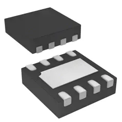
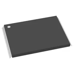
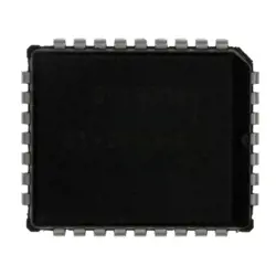
画像は参照用のみです。
PC28F128J3F75B
NOR Flash Parallel NOR Flash(Micron), 128Mb, 3V, 75ns, Uniform Blocks, -40 to 85C, 64b BGA, T&R
- メーカー
- Mfr。パート #PC28F128J3F75B
- パッケージ
- データシート PC28F128J3F75B DataSheet
- 在庫中10080
100% オリジナル &新しい
出荷の準備ができている24時間
365日の保証
RFQおよびもっと割引を得る
仕様
| Packaging | Cut Tape |
| Standard Pack Qty | 2000 |
概要
Description
Key features include:
1. Interface: It supports a parallel interface, facilitating easy integration into various systems.
2. Performance: The chip offers fast read and write speeds, enhancing overall system performance.
3. Endurance: It has a high program/erase cycle endurance, making it suitable for applications with frequent data updates.
4. Data Retention: The memory ensures data integrity over extended periods, crucial for non-volatile applications.
5. Compatibility: It is designed to be compatible with several existing systems and protocols.
Overall, the PC28F128J3F75B is a reliable choice for applications demanding robust and efficient memory solutions.
Features
1. Architecture: It employs a NAND Flash architecture, enabling high-density memory storage.
2. Interface: The device supports a parallel interface, allowing for easy integration with various microcontrollers and processors.
3. Density: Offers 128Mb of storage capacity, suitable for applications requiring significant data storage.
4. Access Speed: Provides fast read and write speeds, enhancing overall system performance.
5. Endurance: Supports a high number of program/erase cycles (typically around 10,000), making it durable for frequent updates.
6. Data Retention: Ensures data retention of up to 20 years under normal conditions.
7. Block Architecture: Features a block-based structure, allowing for efficient data management and partial erasing.
8. Low Power Consumption: Designed for low power operation, making it suitable for battery-operated devices.
These features make the PC28F128J3F75B ideal for applications in consumer electronics, automotive systems, and industrial controls.
Package
Pinout
- Address Inputs (A0-A21): Used to select memory locations.
- Data Inputs/Outputs (DQ0-DQ7): Bi-directional pins for data transfer.
- Chip Enable (CE#): Activates the chip for read/write operations.
- Write Enable (WE#): Controls write operations.
- Output Enable (OE#): Enables data output on DQ pins.
- Byte/Word Select (B/W#): Selects between byte or word mode.
- Reset (RESET#): Resets the device.
- Vcc and Vss: Power supply and ground connections.
This device provides a density of 128Mb and supports multiple operations, including read, program, and erase functions, making it suitable for various applications in embedded systems.
Manufacturer
Application
Equivalent
出荷
出荷方法私たち
DHL、FedEx、TNT、UPS、またはあなたの選択の他の運送業者を通じてグローバルな出荷サービスを提供します。
出荷料参照(DHL/FedEx):
DHL の: 配送費は25ドル〜45ドル(0.5kg)の範囲で、推定配送時間は2〜5営業日です。
フェデックス: 配送費は25ドル〜40ドル(0.5kg)の範囲で、推定配送時間は3〜7営業日。
UPS の: 配送費は25ドル〜45ドル(0.5kg)の範囲で、推定配送時間は3〜7営業日。
TNT社: 配送費は25ドル〜65ドル(0.5kg)の範囲で、推定配送時間は3〜7営業日。
EMS: 配送料金は30〜50ドル(0.5kg)の範囲で、推定配送時間は7〜15営業日です。
登録航空郵便: 配送費は2〜4ドル(0.1kg)で、推定配送時間は5〜20営業日です。
支払い
Payment Methods
支払い期間は100%前払いです。
現在、下記の支払い方法のみを受け入れています。:
1. ペイパル
2. クレジット・デビットカード
3. ワイヤー 転送
類似
-
![MX25R8035FM1IL0]() MX25R8035FM1IL0
Macronix
-
![MX25V5126FM1I]() MX25V5126FM1I
Macronix
-
![MX25L8035EM2I-10G]() MX25L8035EM2I-10G
Macronix
-
![MX25U51279GXDR00]() MX25U51279GXDR00
Macronix
-
![MX25L2006EM1I-12G]() MX25L2006EM1I-12G
Macronix
-
![MX25U3232FZBI02]() MX25U3232FZBI02
Macronix
-
![MX25L6433FM2I-08G]() MX25L6433FM2I-08G
Macronix
-
![MX25L12833FM2I-10G]() MX25L12833FM2I-10..
Macronix
-
![MX25L12833FZ2I-10G]() MX25L12833FZ2I-10..
Macronix
-
![MX25U25645GXDI00]() MX25U25645GXDI00
Macronix
-
![MX29LV160DTTI-70G]() MX29LV160DTTI-70G
Macronix
-
![MX29F040CQI-70G]() MX29F040CQI-70G
Macronix