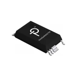
画像は参照用のみです。
P82B715PN
- メーカー
- Mfr。パート #P82B715PN
- パッケージ
- データシート
- 在庫中9976
100% オリジナル &新しい
出荷の準備ができている24時間
365日の保証
RFQおよびもっと割引を得る
仕様
| Packaging | Tube |
| Brand | NXP Semiconductors |
| Product Type | Signal Buffers, Repeaters |
| Factory Pack Quantity:Factory Pack Quantity | 50 |
| Subcategory | Interface ICs |
| Interface Type | I2C/Logic |
| Supply Voltage - Min | 4.5 V |
| Supply Voltage - Max | 12 V |
| Minimum Operating Temperature | - 40 C |
| Maximum Operating Temperature | + 85 C |
| Mounting Style | SMD/SMT |
| Product | Bus Extenders |
| Type | I2C Bus |
| Operating Supply Voltage | 4.5 V to 12 V |
| Package / Case | SOT-97 |
| Part # Aliases | P82B715PN,112 |
| Propagation Delay Time | 250 ns |
| Pd - Power Dissipation | 300 mW |
| Maximum Clock Frequency | 400 kHz |
| Operating Supply Current | 22 mA |
| Output Current | 60 mA |
| Ciss - Input Capacitance | 10 pF |
概要
Description
The P82B715PN is a dedicated integrated circuit designed to extend the range of I2C (Inter-Integrated Circuit) bus communications. It achieves this by acting as a bus buffer. Operating between the standard I2C bus and a buffered bus, it strengthens the bus signals, allowing for longer cable lengths and more devices to be connected without signal degradation, which is a limitation in standard I2C setups.
Key features include the ability to drive large bus capacitances, improving communication over extended distances. The device is typically used in applications requiring reliable data transfer over longer cables, such as industrial automation and complex electronic systems.
The P82B715PN operates by converting the I2C bus signals into buffered levels that can drive more cable length and capacitance. However, the buffered side of the bus requires careful consideration in terms of electrical characteristics and loading to ensure proper function.
Overall, the P82B715PN is an essential component for engineers looking to expand the capabilities of I2C buses in complex and extensive electronic systems.
Features
The P82B715PN is a bi-directional I2C bus extender that facilitates communication over longer distances, typically extending the range of I2C buses beyond the standard limitations. Key features include:
1. I2C Compatibility: Supports I2C and SMBus protocols, allowing for seamless integration with existing systems.
2. Range Extension: By using this extender, you can extend the I2C bus length significantly, accommodating applications where longer cables are required.
3. Voltage Level Shifting: Capable of interfacing devices operating at different voltage levels, making it versatile for mixed-voltage environments.
4. High-Speed Operation: Supports data transfer rates up to 400 kHz, suitable for high-speed I2C applications.
5. Minimal Propagation Delay: Ensures fast communication with minimal delay, usually in the nanosecond range.
6. Wide Supply Voltage Range: Operates over a wide voltage range, typically from 3V to 15V, providing flexibility in various applications.
7. Low Power Consumption: Designed to consume minimal power, making it suitable for battery-operated devices.
8. Robust Performance: Built to handle capacitive loads, improving performance over long cable runs.
These features make the P82B715PN a powerful solution for extending I2C bus capabilities in various industrial and consumer electronics applications.
Package
The P82B715PN is an I2C bus extender with a DIP (Dual In-line Package) type, specifically an 8-pin through-hole package. This package type is commonly used for prototyping and easy integration into breadboards or PCBs.
Pinout
The P82B715PN is an integrated circuit used to extend the range of I²C and SMBus signals. It typically comes in an 8-pin DIP (Dual In-line Package) configuration. Here’s a brief description of its pin functions:
1. VCC (Pin 1): Power supply pin, typically connected to 3.3V or 5V.
2. SDA (Pin 2): Serial Data Line for I²C communication.
3. SCL (Pin 3): Serial Clock Line for I²C communication.
4. GND (Pin 4): Ground connection.
5. SDAIN (Pin 5): Input for serial data from the local I²C bus.
6. SCLIN (Pin 6): Input for serial clock from the local I²C bus.
7. SDAOUT (Pin 7): Output for serial data to the remote I²C bus.
8. SCLOUT (Pin 8): Output for serial clock to the remote I²C bus.
The P82B715PN enables longer bus lengths by buffering the I²C data and clock signals, improving their driving capability and allowing communication over greater distances without signal degradation.
Manufacturer
The P82B715PN is manufactured by NXP Semiconductors. NXP is a global semiconductor company headquartered in Eindhoven, Netherlands. It specializes in the design and manufacturing of a wide range of semiconductor products, including microcontrollers, processors, sensors, and communication infrastructure components. NXP serves various industries, including automotive, industrial, mobile, and communication infrastructure, providing solutions for secure connectivity, smart cities, and the Internet of Things (IoT).
Application
The P82B715PN is a dual bidirectional I2C bus buffer that extends the range and capacitance drive capability of the I2C bus. It is used in applications requiring long-distance I2C communication, including industrial automation, building automation, and communication systems. It facilitates communication between microcontrollers and peripherals over extended distances, improving the reliability and performance of I2C networks in complex systems.
Equivalent
The P82B715PN chip is a bus extender designed for I2C and SMBus systems. Equivalent products include the PCA9600, PCA9617A, and TCA9617A from NXP, TI's TCA9517, and the LTC4311 from Analog Devices. It's important to compare datasheets for compatibility in specific applications.
出荷
出荷方法私たち
DHL、FedEx、TNT、UPS、またはあなたの選択の他の運送業者を通じてグローバルな出荷サービスを提供します。
出荷料参照(DHL/FedEx):
DHL の: 配送費は25ドル〜45ドル(0.5kg)の範囲で、推定配送時間は2〜5営業日です。
フェデックス: 配送費は25ドル〜40ドル(0.5kg)の範囲で、推定配送時間は3〜7営業日。
UPS の: 配送費は25ドル〜45ドル(0.5kg)の範囲で、推定配送時間は3〜7営業日。
TNT社: 配送費は25ドル〜65ドル(0.5kg)の範囲で、推定配送時間は3〜7営業日。
EMS: 配送料金は30〜50ドル(0.5kg)の範囲で、推定配送時間は7〜15営業日です。
登録航空郵便: 配送費は2〜4ドル(0.1kg)で、推定配送時間は5〜20営業日です。
支払い
Payment Methods
支払い期間は100%前払いです。
現在、下記の支払い方法のみを受け入れています。:
1. ペイパル
2. クレジット・デビットカード
3. ワイヤー 転送
類似
-
![MX29F400CBTI-70G]() MX29F400CBTI-70G
Macronix
-
![MX25V16066M1I02]() MX25V16066M1I02
Macronix
-
![MX25R6435FBDIL0]() MX25R6435FBDIL0
Macronix
-
![MX25L25673GMI-08G]() MX25L25673GMI-08G
Macronix
-
![MX25U51279GXDR00]() MX25U51279GXDR00
Macronix
-
![MX25U6435FM2I-10G]() MX25U6435FM2I-10G
Macronix
-
![MX25L12833FM2I-10G]() MX25L12833FM2I-10..
Macronix
-
![MX29LV160DTTI-70G]() MX29LV160DTTI-70G
Macronix
-
![MX25L25645GXDI-08G]() MX25L25645GXDI-08..
Macronix
-
![MX30LF4G18AC-TI]() MX30LF4G18AC-TI
Macronix
-
![MX66U1G45GMI00]() MX66U1G45GMI00
Macronix
-
![MX25L6473FM2I-08G]() MX25L6473FM2I-08G
Macronix