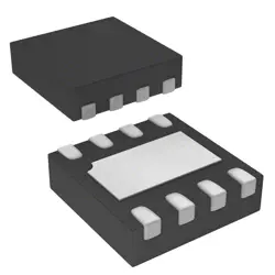
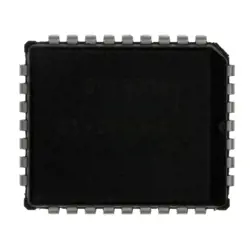
画像は参照用のみです。
OP249GS
IC OPAMP JFET 2 CIRCUIT 8SOIC
- メーカー
- Mfr。パート #OP249GS
- パッケージ SOIC-8
- データシート OP249GS DataSheet
- 在庫中6211
100% オリジナル &新しい
出荷の準備ができている24時間
365日の保証
RFQおよびもっと割引を得る
仕様
| Package | Tube,Tube |
| ProductStatus | Obsolete |
| AmplifierType | J-FET |
| NumberofCircuits | 2 |
| SlewRate | 22V/µs |
| GainBandwidthProduct | 4.7 MHz |
| Current-InputBias | 30 pA |
| Voltage-InputOffset | 400 µV |
| Current-Supply | 5.6mA |
| Current-Output/Channel | 36 mA |
| Voltage-SupplySpan(Min) | 9 V |
| Voltage-SupplySpan(Max) | 36 V |
| OperatingTemperature | -40°C ~ 85°C |
| MountingType | Surface Mount |
| Package/Case | 8-SOIC (0.154, 3.90mm Width) |
概要
Description
OP249GS is a course that typically focuses on the integration of various scientific principles, particularly in the fields of organic chemistry and materials science. It aims to provide students with a foundational understanding of the properties, synthesis, and applications of organic compounds and polymers. The curriculum often emphasizes hands-on laboratory experience, theoretical knowledge, and real-world applications, preparing students for careers in research, industry, or further studies. Key topics may include reaction mechanisms, polymerization techniques, characterization methods, and sustainability in material development. Overall, OP249GS serves as a critical gateway for students pursuing advanced studies in chemistry and related disciplines.
Features
The OP249GS is a precision operational amplifier known for its low offset voltage and low noise characteristics. Key features include:
1. Low Offset Voltage: Typically 25 µV, ensuring high accuracy in applications.
2. Low Noise: With a voltage noise density of 0.4 µV/√Hz, it performs well in sensitive applications.
3. High Slew Rate: Approximately 0.3 V/µs, allowing for fast signal processing.
4. Rail-to-Rail Output: Provides output voltage swing close to the supply rails, maximizing dynamic range.
5. Wide Supply Voltage Range: Operates from a single 3 V to ±15 V supply, offering flexibility in design.
6. Low Input Bias Current: Typically 10 pA, suitable for high-impedance applications.
7. High Gain Bandwidth Product: Around 1 MHz, supporting a variety of applications.
8. Package Options: Available in various packages, including surface-mount options for compact designs.
These features make the OP249GS ideal for instrumentation, data acquisition, and signal conditioning applications.
Package
The OP249GS is packaged in a 8-pin SOIC (Small Outline Integrated Circuit) format.
Pinout
The OP249GS is a precision operational amplifier with a total of 8 pins in a standard SOIC-8 package. Here are the pin functions:
1. 1 (Offset Null): Used for offset voltage adjustment.
2. 2 (Inverting Input, -): The inverting input terminal.
3. 3 (Non-Inverting Input, +): The non-inverting input terminal.
4. 4 (V-): Negative power supply voltage.
5. 5 (Output): The output of the operational amplifier.
6. 6 (NC): No connection (not used).
7. 7 (V+): Positive power supply voltage.
8. 8 (Comp): Compensation pin for stability.
The OP249GS is designed for low offset voltage, low drift, and high precision in various applications, including signal conditioning and instrumentation.
Manufacturer
The OP249GS is manufactured by Analog Devices, Inc. Analog Devices is a multinational semiconductor company that specializes in data conversion, signal processing, and amplification technologies. Founded in 1965, the company is headquartered in Norwood, Massachusetts, and is recognized for its innovation in high-performance analog, mixed-signal, and digital signal processing (DSP) integrated circuits. Analog Devices serves various industries, including telecommunications, automotive, healthcare, aerospace, and consumer electronics, providing solutions that enhance the performance of electronic systems. The OP249GS itself is a precision operational amplifier known for its low offset voltage and low noise characteristics, making it suitable for applications requiring high accuracy and stability.
Application
The OP249GS is a precision operational amplifier used in various applications, including medical instrumentation, industrial automation, signal conditioning, and sensor applications. It is suitable for low-noise and low-drift tasks, making it ideal for audio equipment, data acquisition systems, and feedback loops in control systems. Its high accuracy and stability also benefit precision measurement instruments.
Equivalent
The OP249GS is a precision operational amplifier. Equivalent products include the LT1111, AD711, TLV2371, and OPA227. Ensure that equivalent specifications such as supply voltage, bandwidth, input offset voltage, and noise are compatible for your specific application. Always consult datasheets for detailed comparisons.
出荷
出荷方法私たち
DHL、FedEx、TNT、UPS、またはあなたの選択の他の運送業者を通じてグローバルな出荷サービスを提供します。
出荷料参照(DHL/FedEx):
DHL の: 配送費は25ドル〜45ドル(0.5kg)の範囲で、推定配送時間は2〜5営業日です。
フェデックス: 配送費は25ドル〜40ドル(0.5kg)の範囲で、推定配送時間は3〜7営業日。
UPS の: 配送費は25ドル〜45ドル(0.5kg)の範囲で、推定配送時間は3〜7営業日。
TNT社: 配送費は25ドル〜65ドル(0.5kg)の範囲で、推定配送時間は3〜7営業日。
EMS: 配送料金は30〜50ドル(0.5kg)の範囲で、推定配送時間は7〜15営業日です。
登録航空郵便: 配送費は2〜4ドル(0.1kg)で、推定配送時間は5〜20営業日です。
支払い
Payment Methods
支払い期間は100%前払いです。
現在、下記の支払い方法のみを受け入れています。:
1. ペイパル
2. クレジット・デビットカード
3. ワイヤー 転送
類似
-
![MX25L3233FZBI-08Q]() MX25L3233FZBI-08Q
Macronix
-
![MX25V1635FZNI]() MX25V1635FZNI
Macronix
-
![MX29F400CBTI-70G]() MX29F400CBTI-70G
Macronix
-
![MX66U1G45GXDI00]() MX66U1G45GXDI00
Macronix
-
![MX25V5126FM1I]() MX25V5126FM1I
Macronix
-
![MX25V2033FM1I]() MX25V2033FM1I
Macronix
-
![MX25V16066M2I02]() MX25V16066M2I02
Macronix
-
![MX25R6435FBDIL0]() MX25R6435FBDIL0
Macronix
-
![MX25U51279GXDR00]() MX25U51279GXDR00
Macronix
-
![MX25U3232FZBI02]() MX25U3232FZBI02
Macronix
-
![MX25L12833FZNI-10G]() MX25L12833FZNI-10..
Macronix
-
![MX29F040CQI-70G]() MX29F040CQI-70G
Macronix