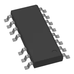
画像は参照用のみです。
NVMFWS2D9N04XMT1G
SINGLE N-CHANNEL POWER MOSFET 40
- メーカー
- Mfr。パート #NVMFWS2D9N04XMT1G
- パッケージ
- データシート NVMFWS2D9N04XMT1G DataSheet
- 在庫中7276
100% オリジナル &新しい
出荷の準備ができている24時間
365日の保証
RFQおよびもっと割引を得る
仕様
| Part Status | Active |
| FET Type | N-Channel |
| Technology | MOSFET (Metal Oxide) |
| Drain to Source Voltage (Vdss) | 40 V |
| Current - Continuous Drain (Id) @ 25°C | 25A (Ta), 94A (Tc) |
| Drive Voltage (Max Rds On, Min Rds On) | 10V |
| Rds On (Max) @ Id, Vgs | 3.1mOhm @ 20A, 10V |
| Vgs(th) (Max) @ Id | 3.5V @ 40µA |
| Gate Charge (Qg) (Max) @ Vgs | 15.7 nC @ 10 V |
| Vgs (Max) | ±20V |
| Input Capacitance (Ciss) (Max) @ Vds | 1000 pF @ 25 V |
| Power Dissipation (Max) | 50W (Tc) |
| Operating Temperature | -55°C ~ 175°C (TJ) |
| Grade | Automotive |
| Qualification | AEC-Q101 |
| Mounting Type | Surface Mount, Wettable Flank |
| Supplier Device Package | 5-DFNW (4.9x5.9) (8-SOFL-WF) |
| Package / Case | 8-PowerTDFN, 5 Leads |
| Base Product Number | NVMFWS |
概要
Description
NVMFWS2D9N04XMT1G is a specific part number for a memory component, typically a flash memory device, produced by a semiconductor manufacturer. This component is part of a non-volatile memory family, indicating it retains data even when power is removed. The “2D” in the part number may refer to a specific architecture or configuration, while the “9N04X” may denote technical specifications such as density, speed, or interface type.
These devices are commonly used in various applications, including consumer electronics, automotive systems, and industrial equipment, where reliable data storage is crucial. Understanding the specifications of such components is essential for engineers and designers selecting the appropriate memory solutions for their projects. For more detailed information, consulting the manufacturer's datasheet is recommended, as it provides specifics on pin configuration, electrical characteristics, and operational guidelines.
These devices are commonly used in various applications, including consumer electronics, automotive systems, and industrial equipment, where reliable data storage is crucial. Understanding the specifications of such components is essential for engineers and designers selecting the appropriate memory solutions for their projects. For more detailed information, consulting the manufacturer's datasheet is recommended, as it provides specifics on pin configuration, electrical characteristics, and operational guidelines.
Features
The NVMFWS2D9N04XMT1G is a type of MOSFET (Metal-Oxide-Semiconductor Field-Effect Transistor) designed for power management applications. Key features include:
1. Voltage Rating: Typically operates at high voltages, making it suitable for various applications.
2. Low On-State Resistance (RDS(on)): This characteristic minimizes power loss during operation, enhancing efficiency.
3. High Switching Speed: Facilitates quick switching for better performance in high-frequency applications.
4. Thermal Performance: Designed to handle elevated temperatures, ensuring reliability and stability under load.
5. Compact Package: Often comes in a small footprint, aiding in space-saving designs in electronic applications.
6. Applications: Commonly used in DC-DC converters, power supplies, and motor drives.
Overall, the NVMFWS2D9N04XMT1G is suited for applications requiring efficient power management and thermal stability.
Package
The NVMFWS2D9N04XMT1G is packaged in a TDFN (Thin Dual Flat No-lead) format, which is a small, surface-mounted package ideal for applications requiring compact design and efficient thermal performance.
Pinout
The NVMFWS2D9N04XMT1G is a 4Mb (512K x 8) NAND Flash memory device. It typically features a 8-pin configuration. The pin functions are as follows:
1. CE# (Chip Enable) - Activates the device.
2. RE# (Read Enable) - Enables reading data from the memory.
3. WE# (Write Enable) - Enables writing data to the memory.
4. ALE (Address Latch Enable) - Latches the address during read/write operations.
5. CLE (Command Latch Enable) - Latches commands sent to the memory.
6. DQ0-DQ7 (Data Input/Output) - Bidirectional data pins for input and output.
7. VCC - Power supply pin.
8. GND - Ground pin.
This device is typically used in various applications for data storage, including consumer electronics and embedded systems.
Manufacturer
The manufacturer of the NVMFWS2D9N04XMT1G is Nexperia. Nexperia is a global semiconductor company that specializes in the production of discrete, logic, and MOSFET components. Formed as a spin-off from NXP Semiconductors in 2017, Nexperia focuses on providing high-performance semiconductor solutions for various applications, including automotive, industrial, and consumer electronics. The company is known for its commitment to high quality, reliability, and efficiency in manufacturing, catering to a wide range of industries with its extensive portfolio of products.
Application
The NVMFWS2D9N04XMT1G is a high-performance N-channel MOSFET primarily used in power management applications. Its application areas include DC-DC converters, power supply units, motor drivers, and battery management systems. It is ideal for switching applications due to its low on-resistance and high efficiency, making it suitable for consumer electronics, automotive systems, and industrial applications.
Equivalent
The NVMFWS2D9N04XMT1G is a power MOSFET. Equivalent products include the NVMFS5C604NL, BSS139, and IRLZ44N. It's important to verify specifications such as voltage, current rating, and R_DS(on) for compatibility in specific applications. Always consult datasheets for detailed comparisons.
出荷
出荷方法私たち
DHL、FedEx、TNT、UPS、またはあなたの選択の他の運送業者を通じてグローバルな出荷サービスを提供します。
出荷料参照(DHL/FedEx):
DHL の: 配送費は25ドル〜45ドル(0.5kg)の範囲で、推定配送時間は2〜5営業日です。
フェデックス: 配送費は25ドル〜40ドル(0.5kg)の範囲で、推定配送時間は3〜7営業日。
UPS の: 配送費は25ドル〜45ドル(0.5kg)の範囲で、推定配送時間は3〜7営業日。
TNT社: 配送費は25ドル〜65ドル(0.5kg)の範囲で、推定配送時間は3〜7営業日。
EMS: 配送料金は30〜50ドル(0.5kg)の範囲で、推定配送時間は7〜15営業日です。
登録航空郵便: 配送費は2〜4ドル(0.1kg)で、推定配送時間は5〜20営業日です。
支払い
Payment Methods
支払い期間は100%前払いです。
現在、下記の支払い方法のみを受け入れています。:
1. ペイパル
2. クレジット・デビットカード
3. ワイヤー 転送
類似
-
![MX25R8035FM1IL0]() MX25R8035FM1IL0
Macronix
-
![MX25L3233FZBI-08Q]() MX25L3233FZBI-08Q
Macronix
-
![MX25L3233FM1I-08Q]() MX25L3233FM1I-08Q
Macronix
-
![MX25V5126FM1I]() MX25V5126FM1I
Macronix
-
![MX25V4035FZUI]() MX25V4035FZUI
Macronix
-
![MX25V16066M1I02]() MX25V16066M1I02
Macronix
-
![MX25R1635FZUIH0]() MX25R1635FZUIH0
Macronix
-
![MX25V1635FM2I]() MX25V1635FM2I
Macronix
-
![MX25L12833FZNI-10G]() MX25L12833FZNI-10..
Macronix
-
![MX25L12835FZ2I-10G]() MX25L12835FZ2I-10..
Macronix
-
![MX29LV160DTTI-70G]() MX29LV160DTTI-70G
Macronix
-
![MX25L25735FMI-10G]() MX25L25735FMI-10G
Macronix