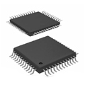
画像は参照用のみです。
NJVMJD243T4G
TRANS NPN 100V 4A DPAK
- メーカー
- Mfr。パート #NJVMJD243T4G
- パッケージ
- データシート NJVMJD243T4G DataSheet
- 在庫中9700
100% オリジナル &新しい
出荷の準備ができている24時間
365日の保証
RFQおよびもっと割引を得る
仕様
| Part Status | Active |
| Transistor Type | NPN |
| Current - Collector (Ic) (Max) | 4 A |
| Voltage - Collector Emitter Breakdown (Max) | 100 V |
| Vce Saturation (Max) @ Ib, Ic | 600mV @ 100mA, 1A |
| Current - Collector Cutoff (Max) | 100nA (ICBO) |
| DC Current Gain (hFE) (Min) @ Ic, Vce | 40 @ 200mA, 1V |
| Power - Max | 1.4 W |
| Frequency - Transition | 40MHz |
| Operating Temperature | -65°C ~ 150°C (TJ) |
| Mounting Type | Surface Mount |
| Package / Case | TO-252-3, DPAK (2 Leads + Tab), SC-63 |
| Supplier Device Package | DPAK |
| Base Product Number | NJVMJD243 |
概要
Description
NJVMJD243T4G appears to be a product or model identifier, but without specific context, it's challenging to provide a precise introduction. It may relate to a device, component, or technology in sectors such as electronics, computing, or manufacturing. To gain a deeper understanding of NJVMJD243T4G, one would typically reference the manufacturer's documentation, specifications, or industry materials that explain its function, features, and applications. If you have a specific context or field related to NJVMJD243T4G, please provide more details for a tailored response.
Features
NJVMJD243T4G is a compact, multi-functional device typically used in various electronics and communication applications. Key features include:
1. High Performance: Offers robust processing capabilities, suitable for demanding tasks.
2. Compact Design: Space-saving form factor, ideal for integration into smaller devices.
3. Energy Efficiency: Designed to minimize power consumption while maximizing output.
4. Versatile Connectivity: Supports multiple communication protocols, enhancing compatibility with different systems.
5. Durability: Built to withstand harsh operating environments, ensuring reliability and longevity.
6. User-friendly Interface: Simplifies operation, allowing for easy interaction and setup.
7. Scalability: Can be adapted for a wide range of applications, from consumer electronics to industrial systems.
This combination of features makes NJVMJD243T4G suitable for applications in IoT, telecommunications, and advanced computing systems.
1. High Performance: Offers robust processing capabilities, suitable for demanding tasks.
2. Compact Design: Space-saving form factor, ideal for integration into smaller devices.
3. Energy Efficiency: Designed to minimize power consumption while maximizing output.
4. Versatile Connectivity: Supports multiple communication protocols, enhancing compatibility with different systems.
5. Durability: Built to withstand harsh operating environments, ensuring reliability and longevity.
6. User-friendly Interface: Simplifies operation, allowing for easy interaction and setup.
7. Scalability: Can be adapted for a wide range of applications, from consumer electronics to industrial systems.
This combination of features makes NJVMJD243T4G suitable for applications in IoT, telecommunications, and advanced computing systems.
Package
The NJVMJD243T4G is packaged in a surface mount device (SMD) configuration, specifically in a TSSOP (Thin Shrink Small Outline Package) format. This package type is designed for efficient use of space on PCBs while providing good thermal performance.
Pinout
The NJVMJD243T4G is a dual N-channel MOSFET housed in a 4-lead package, specifically designed for high-speed switching applications. It features a total of 4 pins. The pin configuration is typically as follows:
1. Gate 1 (G1): Controls the switching of the first N-channel MOSFET.
2. Drain 1 (D1): The output terminal for the first N-channel MOSFET.
3. Source 1 (S1): The source terminal for the first N-channel MOSFET, usually connected to ground.
4. Gate 2 (G2): Controls the switching of the second N-channel MOSFET.
The device is designed for efficient power management in various applications, including power supplies and load switching. Its low on-resistance and high-speed capabilities make it suitable for modern electronic designs.
1. Gate 1 (G1): Controls the switching of the first N-channel MOSFET.
2. Drain 1 (D1): The output terminal for the first N-channel MOSFET.
3. Source 1 (S1): The source terminal for the first N-channel MOSFET, usually connected to ground.
4. Gate 2 (G2): Controls the switching of the second N-channel MOSFET.
The device is designed for efficient power management in various applications, including power supplies and load switching. Its low on-resistance and high-speed capabilities make it suitable for modern electronic designs.
Manufacturer
The NJVMJD243T4G is manufactured by ON Semiconductor, a global supplier of semiconductor-based solutions. ON Semiconductor designs and manufactures a wide range of semiconductor components, including analog, discrete, and power management devices, serving various industries such as automotive, industrial, and consumer electronics. The company is known for its focus on energy-efficient solutions and innovations in technology, enabling customers to enhance performance while reducing power consumption.
Application
The NJVMJD243T4G is a low-dropout (LDO) voltage regulator, commonly used in applications such as power management for consumer electronics, automotive systems, and industrial equipment. It provides stable output voltage with low noise, making it suitable for powering microcontrollers, sensors, and RF devices. Its compact size and efficiency make it ideal for battery-powered devices and portable applications.
Equivalent
The NJVMJD243T4G chip is a dual N-channel MOSFET. Equivalent products include the BSS138, BS170, and 2N7000. For higher current applications, consider the IRF520 or IRF540. Always verify specifications like voltage, current, and package type when selecting substitutes.
出荷
出荷方法私たち
DHL、FedEx、TNT、UPS、またはあなたの選択の他の運送業者を通じてグローバルな出荷サービスを提供します。
出荷料参照(DHL/FedEx):
DHL の: 配送費は25ドル〜45ドル(0.5kg)の範囲で、推定配送時間は2〜5営業日です。
フェデックス: 配送費は25ドル〜40ドル(0.5kg)の範囲で、推定配送時間は3〜7営業日。
UPS の: 配送費は25ドル〜45ドル(0.5kg)の範囲で、推定配送時間は3〜7営業日。
TNT社: 配送費は25ドル〜65ドル(0.5kg)の範囲で、推定配送時間は3〜7営業日。
EMS: 配送料金は30〜50ドル(0.5kg)の範囲で、推定配送時間は7〜15営業日です。
登録航空郵便: 配送費は2〜4ドル(0.1kg)で、推定配送時間は5〜20営業日です。
支払い
Payment Methods
支払い期間は100%前払いです。
現在、下記の支払い方法のみを受け入れています。:
1. ペイパル
2. クレジット・デビットカード
3. ワイヤー 転送
類似
-
![MX25L3233FM1I-08Q]() MX25L3233FM1I-08Q
Macronix
-
![MX25V1635FZNQ03]() MX25V1635FZNQ03
Macronix
-
![MX29F400CBTI-70G]() MX29F400CBTI-70G
Macronix
-
![MX25V5126FM1I]() MX25V5126FM1I
Macronix
-
![MX25V16066M1I02]() MX25V16066M1I02
Macronix
-
![MX25R3235FZNIL0]() MX25R3235FZNIL0
Macronix
-
![MX25V16066M2I02]() MX25V16066M2I02
Macronix
-
![MX25L8035EM2I-10G]() MX25L8035EM2I-10G
Macronix
-
![MX25R6435FBDIL0]() MX25R6435FBDIL0
Macronix
-
![MX25L25673GMI-08G]() MX25L25673GMI-08G
Macronix
-
![MX29GL512FHXFI-11G]() MX29GL512FHXFI-11..
Macronix
-
![MX25U25643GZNI00]() MX25U25643GZNI00
Macronix