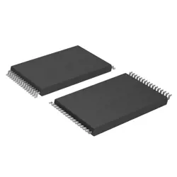
画像は参照用のみです。
NCP5183DR2G
IC GATE DRVR HALF-BRIDGE 8SOIC
- メーカー
- Mfr。パート #NCP5183DR2G
- パッケージ 8-SOIC
- データシート
- 在庫中7494
100% オリジナル &新しい
出荷の準備ができている24時間
365日の保証
RFQおよびもっと割引を得る
仕様
| Package | Tape & Reel (TR),Cut Tape (CT) |
| ProductStatus | Active |
| DrivenConfiguration | Half-Bridge |
| ChannelType | Independent |
| NumberofDrivers | 2 |
| GateType | N-Channel MOSFET |
| Voltage-Supply | 9V ~ 18V |
| LogicVoltage-VILVIH | 1.2V, 2.5V |
| Current-PeakOutput(SourceSink) | 4.3A, 4.3A |
| InputType | Non-Inverting |
| HighSideVoltage-Max(Bootstrap) | 600 V |
| Rise/FallTime(Typ) | 12ns, 12ns |
| OperatingTemperature | -40°C ~ 125°C (TJ) |
| MountingType | Surface Mount |
| Package/Case | 8-SOIC (0.154, 3.90mm Width) |
概要
Description
NCP5183DR2G is an ON Semiconductor buck (step-down) switching regulator IC. It is used to convert a higher input voltage into a stable, lower output for microprocessors, microcontrollers, and other loads, often in automotive and industrial applications. The DR2G package denotes a compact RoHS SMD package.
Key points:
- Regulation: PWM switching regulator with an external inductor and energy storage components.
- Output: adjustable via a feedback resistor divider (and may have a fixed option depending on variant); controlled by an enable/soft-start mechanism.
- Protection: overcurrent/short-circuit protection and thermal shutdown.
- Efficiency: designed for high efficiency across load conditions.
- External components: requires inductor, catch diode (if not using a synchronous design), input/output capacitors, and feedback network.
- Applications: power supplies for PMICs, MCU rails, automotive and industrial electronics.
For exact electrical specifications (input range, output range, switching frequency, current capability) and schematic/app notes, consult the NCP5183DR2G datasheet and product page.
Features
NCP5183DR2G features (On Semiconductor) typically include:
- High-efficiency buck DC-DC converter with integrated high-side MOSFET
- Wide input voltage range (suitable for various apps)
- Adjustable output via external resistor divider
- Fixed switching frequency with current‑mode PWM control (and PWM/PFM modes)
- Soft-start to limit inrush
- Enable/disable control
- Overcurrent/short-circuit protection
- Thermal shutdown and thermal overload protection
- UVLO (undervoltage lockout) protection
- Optional protection features (e.g., overvoltage)
- Pin-compatible, compact DR2G package
Note: exact electrical specs (input range, output range, frequency, efficiency) vary by variant. Please consult the NCP5183DR2G datasheet for precise data.
Package
DFN-8 package: 2×2 mm with exposed pad (RoHS-compliant).
Pinout
- Pin count: 8 pins (DR2G package).
- Function: Buck (step-down) switching regulator with an integrated high-side switch; provides a regulated output from Vin via external feedback; includes enable/shutdown.
- Function: Buck (step-down) switching regulator with an integrated high-side switch; provides a regulated output from Vin via external feedback; includes enable/shutdown.
Manufacturer
NCP5183DR2G is manufactured by ON Semiconductor (onsemi). ON Semiconductor is a US-based global semiconductor company that designs and produces energy-efficient power management ICs, analog and discrete devices for automotive, industrial, communications, and consumer markets. It was spun off from Motorola and is publicly traded (NASDAQ: ON).
Application
Application areas:
- High-efficiency synchronous buck regulator for point-of-load power in low-voltage, battery-powered systems
- Mobile/consumer devices (smartphones, tablets, wearables); notebooks and embedded systems
- Automotive and industrial electronics (1.8–5 V rails)
- Power supplies and USB chargers; IoT and microcontroller/SoC rails
出荷
出荷方法私たち
DHL、FedEx、TNT、UPS、またはあなたの選択の他の運送業者を通じてグローバルな出荷サービスを提供します。
出荷料参照(DHL/FedEx):
DHL の: 配送費は25ドル〜45ドル(0.5kg)の範囲で、推定配送時間は2〜5営業日です。
フェデックス: 配送費は25ドル〜40ドル(0.5kg)の範囲で、推定配送時間は3〜7営業日。
UPS の: 配送費は25ドル〜45ドル(0.5kg)の範囲で、推定配送時間は3〜7営業日。
TNT社: 配送費は25ドル〜65ドル(0.5kg)の範囲で、推定配送時間は3〜7営業日。
EMS: 配送料金は30〜50ドル(0.5kg)の範囲で、推定配送時間は7〜15営業日です。
登録航空郵便: 配送費は2〜4ドル(0.1kg)で、推定配送時間は5〜20営業日です。
支払い
Payment Methods
支払い期間は100%前払いです。
現在、下記の支払い方法のみを受け入れています。:
1. ペイパル
2. クレジット・デビットカード
3. ワイヤー 転送
類似
-
![MX25R8035FM1IL0]() MX25R8035FM1IL0
Macronix
-
![MX25V5126FM1I]() MX25V5126FM1I
Macronix
-
![MX25V16066M1I02]() MX25V16066M1I02
Macronix
-
![MX25R3235FZNIL0]() MX25R3235FZNIL0
Macronix
-
![MX30LF2G28AD-TI]() MX30LF2G28AD-TI
Macronix
-
![MX25L8035EM2I-10G]() MX25L8035EM2I-10G
Macronix
-
![MX25L2006EM1I-12G]() MX25L2006EM1I-12G
Macronix
-
![MX25L6433FM2I-08G]() MX25L6433FM2I-08G
Macronix
-
![MX25U25645GXDI00]() MX25U25645GXDI00
Macronix
-
![MX29F040CQI-70G]() MX29F040CQI-70G
Macronix
-
![MX29F040CTI-70G]() MX29F040CTI-70G
Macronix
-
![MX29LV640ETTI-70G]() MX29LV640ETTI-70G
Macronix