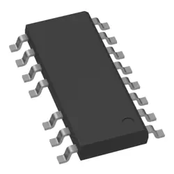
画像は参照用のみです。
NB3L553DR2G
IC CLK BUFFER 1:4 200MHZ 8SOIC
- メーカー
- Mfr。パート #NB3L553DR2G
- パッケージ SOIC-8
- データシート
- 在庫中7076
100% オリジナル &新しい
出荷の準備ができている24時間
365日の保証
RFQおよびもっと割引を得る
仕様
| Package | Tape & Reel (TR),Cut Tape (CT) |
| ProductStatus | Active |
| Type | Fanout Buffer (Distribution) |
| NumberofCircuits | 1 |
| Ratio-Input:Output | 1:4 |
| Differential-Input:Output | No/No |
| Input | LVCMOS, LVTTL |
| Output | LVCMOS, LVTTL |
| Frequency-Max | 200 MHz |
| Voltage-Supply | 2.375V ~ 5.25V |
| OperatingTemperature | -40°C ~ 85°C |
| MountingType | Surface Mount |
| Package/Case | 8-SOIC (0.154, 3.90mm Width) |
概要
Description
The NB3L553DR2G is a high-performance, low-jitter clock generator and distribution device manufactured by ON Semiconductor. It is designed to provide precise clock signals for various applications, including telecommunications, networking, and data communications. This device supports multiple output formats and frequencies, allowing for flexibility in system design.
Key features include low phase noise and low jitter, which are critical for maintaining signal integrity in high-speed data environments. The NB3L553DR2G typically operates from a single power supply and is available in a compact package, making it suitable for space-constrained applications.
It can generate up to four clock outputs, which can be synchronized to a single input clock, ensuring consistent timing across the system. The NB3L553DR2G is ideal for applications requiring reliable clock generation, such as routers, switches, and high-speed data converters. Overall, it is a versatile solution for ensuring accurate timing in electronic systems.
Features
The NB3L553DR2G is a programmable clock generator designed for high-performance applications. Key features include:
1. Output Frequency Range: It supports a wide frequency range, suitable for various applications.
2. Low Jitter Performance: The device offers low phase jitter, enhancing signal integrity for high-speed designs.
3. Multiple Outputs: It provides multiple output clocks, which can be independently configured.
4. Flexible Configuration: The clock generator can be programmed to support different frequency settings through I2C or SPI interfaces.
5. Power Supply: Operates with a low supply voltage, contributing to reduced power consumption.
6. Temperature Stability: Enhanced performance over a wide temperature range, ensuring reliability in diverse environments.
7. Compact Package: Available in a compact package for space-constrained applications.
These features make the NB3L553DR2G suitable for applications in telecommunications, networking, and consumer electronics where precise clocking is essential.
Package
The NB3L553DR2G is packaged in a 8-pin TSSOP (Thin Shrink Small Outline Package). This compact package type is designed for efficient use of PCB space and is suitable for various applications in electronics.
Pinout
The NB3L553DR2G is a high-performance clock generator with a 16-pin TSSOP package. It typically has a pin count of 16. The primary functions of the NB3L553DR2G include generating various output clock frequencies from a single input reference clock, with support for multiple output formats. Key pins include:
1. REFCLK: Input reference clock.
2. OUT: Output clock signals.
3. GND: Ground connection.
4. VDD: Power supply pin.
5. SEL: Frequency select pin to choose different output frequencies.
6. FB: Feedback pin for configuring output frequency.
The device is commonly used in applications requiring precise clock signals, such as in communications, networking, and consumer electronics.
Manufacturer
The manufacturer of the NB3L553DR2G is ON Semiconductor. ON Semiconductor is a global semiconductor company that designs and manufactures a wide range of products, including analog, discrete, and power semiconductors. They serve various sectors such as automotive, industrial, communications, computing, and consumer electronics. The company focuses on developing energy-efficient solutions and technologies that enable customers to create innovative products in an increasingly connected world.
Application
The NB3L553DR2G is a high-performance clock buffer and fanout device primarily used in telecommunications, data centers, and networking applications. Its key areas of application include high-speed data transmission, clock distribution for systems requiring low jitter, and signal integrity enhancement in electronic designs. It is suitable for use in routers, switches, and other communication equipment that require precise timing and synchronization.
Equivalent
The NB3L553DR2G is a low-power clock buffer. Equivalent products include the NXP 74LVC1G123, TI SN74LVC1G124, and ON Semiconductor MC100EP16. Additionally, products like the IDT 5P49V5930 and SiTime SiT9102 can serve similar functions, depending on specific requirements like frequency range and output drive strength. Always check datasheets for compatibility.
出荷
出荷方法私たち
DHL、FedEx、TNT、UPS、またはあなたの選択の他の運送業者を通じてグローバルな出荷サービスを提供します。
出荷料参照(DHL/FedEx):
DHL の: 配送費は25ドル〜45ドル(0.5kg)の範囲で、推定配送時間は2〜5営業日です。
フェデックス: 配送費は25ドル〜40ドル(0.5kg)の範囲で、推定配送時間は3〜7営業日。
UPS の: 配送費は25ドル〜45ドル(0.5kg)の範囲で、推定配送時間は3〜7営業日。
TNT社: 配送費は25ドル〜65ドル(0.5kg)の範囲で、推定配送時間は3〜7営業日。
EMS: 配送料金は30〜50ドル(0.5kg)の範囲で、推定配送時間は7〜15営業日です。
登録航空郵便: 配送費は2〜4ドル(0.1kg)で、推定配送時間は5〜20営業日です。
支払い
Payment Methods
支払い期間は100%前払いです。
現在、下記の支払い方法のみを受け入れています。:
1. ペイパル
2. クレジット・デビットカード
3. ワイヤー 転送
類似
-
![MX25L3233FZBI-08Q]() MX25L3233FZBI-08Q
Macronix
-
![MX25V1635FZNI]() MX25V1635FZNI
Macronix
-
![MX25V5126FM1I]() MX25V5126FM1I
Macronix
-
![MX25V4035FZUI]() MX25V4035FZUI
Macronix
-
![MX25V16066M1I02]() MX25V16066M1I02
Macronix
-
![MX30LF2G28AD-TI]() MX30LF2G28AD-TI
Macronix
-
![MX25L8035EM2I-10G]() MX25L8035EM2I-10G
Macronix
-
![MX29GL512FHXFI-11G]() MX29GL512FHXFI-11..
Macronix
-
![MX25L2006EM1I-12G]() MX25L2006EM1I-12G
Macronix
-
![MX25L12833FM2I-10G]() MX25L12833FM2I-10..
Macronix
-
![MX29F800CBTI-70G]() MX29F800CBTI-70G
Macronix
-
![MX25L25735FMI-10G]() MX25L25735FMI-10G
Macronix