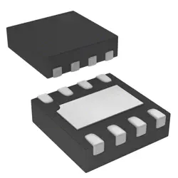
画像は参照用のみです。
MT48LC2M32B2P-6A IT:J
3V~3.6V 64Mbit 167MHz TSOP-86-10.2mm Memory (ICs) RoHS
- メーカー
- Mfr。パート #MT48LC2M32B2P-6A IT:J
- パッケージ
- データシート MT48LC2M32B2P-6A IT:J DataSheet
- 在庫中23249
100% オリジナル &新しい
出荷の準備ができている24時間
365日の保証
RFQおよびもっと割引を得る
仕様
| Packaging | TSOP-86-10.2mm |
| Clock Frequency | 167MHz |
| Memory Size | 64Mbit |
| Operating temperature | -40℃~+85℃ |
| Voltage - Supply | 3V~3.6V |
概要
Description
The MT48LC2M32B2P-6A is a 2 Meg x 32-bit DRAM memory chip from Micron Technology. It is designed for high-density memory applications, providing 64 Megabytes of data storage. This part belongs to the DDR (Double Data Rate) SDRAM family, which allows for faster data transfer rates compared to traditional SDRAM by transferring data on both the rising and falling edges of the clock cycle.
Key features include a 6 ns access time, a wide data bus for increased throughput, and support for various operating modes, making it suitable for applications in computing, networking, and telecommunications. The device operates at a voltage of 3.3V and has a package type of TSOP II, which is standard in many embedded systems. The "IT" in its designation indicates industrial temperature range, ensuring reliability in harsh conditions.
Overall, the MT48LC2M32B2P-6A is ideal for applications requiring stable, high-performance memory solutions.
Features
The MT48LC2M32B2P-6A IT:J is a 2 Meg x 32-bit DDR SDRAM (Dynamic Random Access Memory) chip from Micron Technology. Key features include:
- Density: 64 Megabytes (2M x 32 configuration).
- Speed: Operates at a clock frequency of 166 MHz, with a data rate of 333 MT/s.
- Voltage: Operates at a supply voltage of 2.5V, with I/O levels compatible with 2.5V.
- Package: Available in a 54-ball Fine Pitch Ball Grid Array (FBGA) package, ideal for compact designs.
- Functionality: Supports burst read and write operations, enhancing data throughput.
- Compatibility: Designed for DDR SDRAM applications, suitable for various computing and networking applications.
- Temperature Range: Industrial temperature range, making it suitable for harsh environments.
This component is widely used in embedded systems, telecommunications, and industrial applications where reliability and performance are critical.
Package
The MT48LC2M32B2P-6A IT:J is packaged in a 78-ball TFBGA (Thin Fine Ball Grid Array) format. This type of package is designed for high-density memory applications, providing a compact footprint and efficient thermal performance.
Pinout
The MT48LC2M32B2P-6A IT:J is a 256Mb (32MB) SDRAM memory chip organized as 2M x 32 with a pin count of 54 pins.
### Pin Functions:
1. Address Pins (A0-A11): Used to select the memory location.
2. Data Pins (DQ0-DQ31): Bi-directional data bus for reading and writing data.
3. Control Pins:
- CS: Chip Select, used to enable the chip.
- RAS: Row Address Strobe, activates row access.
- CAS: Column Address Strobe, activates column access.
- WE: Write Enable, controls write operations.
- CLK: Clock input for synchronizing operations.
4. Power and Ground Pins: VDD and VSS for power supply and grounding.
5. Other Pins: Including DQM for data masking, and other auxiliary pins for various functions.
This SDRAM is designed for high-performance applications in computing and telecommunications.
Manufacturer
The manufacturer of the MT48LC2M32B2P-6A IT:J is Micron Technology, Inc. Micron is an American company that specializes in semiconductor manufacturing, particularly in memory and storage solutions. Founded in 1978 and headquartered in Boise, Idaho, Micron produces a wide range of products, including DRAM, NAND flash memory, and solid-state drives. The company serves various markets, including computing, mobile, consumer electronics, and automotive sectors, and is known for its innovation in memory technology. Micron is one of the largest memory manufacturers globally and plays a significant role in the semiconductor industry.
Application
The MT48LC2M32B2P-6A IT:J is a DRAM memory chip commonly used in telecommunications, networking equipment, and industrial applications. It is suitable for devices requiring high-density memory with low power consumption, such as routers, switches, and embedded systems. Its reliability and performance make it ideal for applications in computing, automotive systems, and consumer electronics.
Equivalent
The MT48LC2M32B2P-6A IT:J chip is a DDR2 SDRAM memory chip. Equivalent products include:
1. Hynix HYMD264G728A6
2. Samsung K4T1G164QE
3. Micron MT47H64M16HR-3
Ensure to check the specifications, such as speed, voltage, and package type, for compatibility in your application.
1. Hynix HYMD264G728A6
2. Samsung K4T1G164QE
3. Micron MT47H64M16HR-3
Ensure to check the specifications, such as speed, voltage, and package type, for compatibility in your application.
出荷
出荷方法私たち
DHL、FedEx、TNT、UPS、またはあなたの選択の他の運送業者を通じてグローバルな出荷サービスを提供します。
出荷料参照(DHL/FedEx):
DHL の: 配送費は25ドル〜45ドル(0.5kg)の範囲で、推定配送時間は2〜5営業日です。
フェデックス: 配送費は25ドル〜40ドル(0.5kg)の範囲で、推定配送時間は3〜7営業日。
UPS の: 配送費は25ドル〜45ドル(0.5kg)の範囲で、推定配送時間は3〜7営業日。
TNT社: 配送費は25ドル〜65ドル(0.5kg)の範囲で、推定配送時間は3〜7営業日。
EMS: 配送料金は30〜50ドル(0.5kg)の範囲で、推定配送時間は7〜15営業日です。
登録航空郵便: 配送費は2〜4ドル(0.1kg)で、推定配送時間は5〜20営業日です。
支払い
Payment Methods
支払い期間は100%前払いです。
現在、下記の支払い方法のみを受け入れています。:
1. ペイパル
2. クレジット・デビットカード
3. ワイヤー 転送
類似
-
![MX25V1635FZNI]() MX25V1635FZNI
Macronix
-
![MX25V1635FZNQ03]() MX25V1635FZNQ03
Macronix
-
![MX25V5126FM1I]() MX25V5126FM1I
Macronix
-
![MX25V4035FZUI]() MX25V4035FZUI
Macronix
-
![MX25V2033FM1I]() MX25V2033FM1I
Macronix
-
![MX30LF2G28AD-TI]() MX30LF2G28AD-TI
Macronix
-
![MX25L8035EM2I-10G]() MX25L8035EM2I-10G
Macronix
-
![MX25R6435FBDIL0]() MX25R6435FBDIL0
Macronix
-
![MX25U51279GXDR00]() MX25U51279GXDR00
Macronix
-
![MX25R1635FZUIH0]() MX25R1635FZUIH0
Macronix
-
![MX25U6435FM2I-10G]() MX25U6435FM2I-10G
Macronix
-
![MX25U25645GXDI00]() MX25U25645GXDI00
Macronix