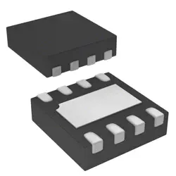
画像は参照用のみです。
MT48LC16M16A2P-6A IT:G
3V~3.6V 256Mbit 167MHz TSOP-54-10.2mm Memory (ICs) RoHS
- メーカー
- Mfr。パート #MT48LC16M16A2P-6A IT:G
- パッケージ
- データシート
- 在庫中6309
100% オリジナル &新しい
出荷の準備ができている24時間
365日の保証
RFQおよびもっと割引を得る
仕様
| Packaging | TSOP-54-10.2mm |
| Clock Frequency | 167MHz |
| Memory Size | 256Mbit |
| Operating temperature | -40℃~+85℃ |
| Voltage - Supply | 3V~3.6V |
概要
Description
The MT48LC16M16A2P-6A IT:G is a 256Mb (16M x 16) DRAM memory chip produced by Micron Technology. It uses a CMOS process and is designed for high-performance applications. This specific model operates at a clock speed of 166 MHz and has a 6 ns access time, making it suitable for various computing tasks.
Key features include:
- Architecture: 16 Meg x 16 bit organization.
- Operating Voltage: Typically operates at 3.3V.
- Temperature Range: Industrial-grade (IT) version supports a temperature range of -40°C to +85°C.
- Package Type: Available in a standard TSOP-II package, facilitating easy integration into systems.
- Data Rates: Designed for synchronous operation, supporting burst mode and interleaved access.
The MT48LC16M16A2P-6A IT:G is commonly used in applications such as networking, telecommunications, and industrial systems where reliability and performance are critical.
Features
The MT48LC16M16A2P-6A IT:G is a 256Mb (16M x 16) DDR SDRAM memory chip designed for high-performance applications. Key features include:
1. Density: 256 Megabits organized as 16 Megabytes x 16 bits.
2. Speed: Operates at a clock frequency of 166 MHz, with a data rate of 333 MT/s.
3. Low Power: IT (Industrial Temperature) grade supports a wide temperature range, typically from -40°C to +95°C, making it suitable for industrial applications.
4. Architecture: It employs a double-data-rate architecture, providing higher bandwidth by transferring data on both rising and falling edges of the clock signal.
5. Interface: The chip features a synchronous interface, which allows for burst accesses to improve performance.
6. Package: Available in a 54-ball FBGA (Fine Ball Grid Array) package for compact designs.
7. Power Supply: Operates at 2.5V for core and 1.8V for I/O.
These features make the MT48LC16M16A2P-6A IT:G suitable for various applications in telecommunications, networking, and industrial environments.
Package
The MT48LC16M16A2P-6A IT:G is typically packaged in a TSOP-II (Thin Small Outline Package) form factor. This package type is commonly used for DRAM devices, providing a compact and efficient layout for integration on printed circuit boards.
Pinout
The MT48LC16M16A2P-6A IT:G is a 256Mb DRAM chip with a pin count of 54. It is organized as 16 Meg x 16 bits and operates on a single 3.3V supply. The major functions of its pins include:
1. Address Inputs (A0-A11): Used for selecting memory locations.
2. Data Inputs/Outputs (DQ0-DQ15): Used for data transfer.
3. Chip Select (CS): Activates the chip for read/write operations.
4. Row Address Strobe (RAS): Used to latch the row address.
5. Column Address Strobe (CAS): Used to latch the column address.
6. Write Enable (WE): Controls write operations.
7. Byte Select (UB, LB): Used for selecting upper or lower bytes during data operations.
8. Clock (CLK): Synchronizes operations.
9. Power (VDD, VSS): Supplies power to the chip.
This DRAM is designed for high-performance applications and features low power consumption, making it suitable for various electronic devices.
Manufacturer
The MT48LC16M16A2P-6A IT:G is manufactured by Micron Technology, Inc. Micron is a global leader in the semiconductor industry, specializing in memory and storage solutions. Founded in 1978 and headquartered in Boise, Idaho, Micron produces a variety of products, including DRAM, NAND flash memory, and solid-state drives (SSDs), serving markets such as computing, mobile, automotive, and industrial applications. The company focuses on innovation and technology advancements in memory products, aiming to meet the growing demands for data storage and processing in various devices. Micron is also recognized for its commitment to sustainability and corporate responsibility in its operations.
Application
The MT48LC16M16A2P-6A IT:G is a DDR SDRAM memory chip commonly used in applications such as telecommunications, networking equipment, embedded systems, and industrial computing. Its features make it suitable for high-performance data processing in devices like servers, routers, and storage solutions, as well as in automotive and aerospace applications, where reliability and durability under extreme conditions are essential.
Equivalent
The MT48LC16M16A2P-6A IT:G chip is a 256MB DDR SDRAM memory chip. Equivalent products include:
1. Hynix HY57V161620C
2. Samsung K4S161622D
3. Elpida EDE5116B2A
4. Micron MT48LC16M16A2P-6A
Ensure compatibility with specifications, such as speed, voltage, and pin configuration, when considering substitutes.
1. Hynix HY57V161620C
2. Samsung K4S161622D
3. Elpida EDE5116B2A
4. Micron MT48LC16M16A2P-6A
Ensure compatibility with specifications, such as speed, voltage, and pin configuration, when considering substitutes.
出荷
出荷方法私たち
DHL、FedEx、TNT、UPS、またはあなたの選択の他の運送業者を通じてグローバルな出荷サービスを提供します。
出荷料参照(DHL/FedEx):
DHL の: 配送費は25ドル〜45ドル(0.5kg)の範囲で、推定配送時間は2〜5営業日です。
フェデックス: 配送費は25ドル〜40ドル(0.5kg)の範囲で、推定配送時間は3〜7営業日。
UPS の: 配送費は25ドル〜45ドル(0.5kg)の範囲で、推定配送時間は3〜7営業日。
TNT社: 配送費は25ドル〜65ドル(0.5kg)の範囲で、推定配送時間は3〜7営業日。
EMS: 配送料金は30〜50ドル(0.5kg)の範囲で、推定配送時間は7〜15営業日です。
登録航空郵便: 配送費は2〜4ドル(0.1kg)で、推定配送時間は5〜20営業日です。
支払い
Payment Methods
支払い期間は100%前払いです。
現在、下記の支払い方法のみを受け入れています。:
1. ペイパル
2. クレジット・デビットカード
3. ワイヤー 転送
類似
-
![MX25V1635FZNI]() MX25V1635FZNI
Macronix
-
![MX66U1G45GXDI00]() MX66U1G45GXDI00
Macronix
-
![MX25V5126FM1I]() MX25V5126FM1I
Macronix
-
![MX25V4035FZUI]() MX25V4035FZUI
Macronix
-
![MX25V16066M1I02]() MX25V16066M1I02
Macronix
-
![MX25R3235FZNIL0]() MX25R3235FZNIL0
Macronix
-
![MX25V16066M2I02]() MX25V16066M2I02
Macronix
-
![MX30LF2G28AD-TI]() MX30LF2G28AD-TI
Macronix
-
![MX25L8035EM2I-10G]() MX25L8035EM2I-10G
Macronix
-
![MX25U3232FZBI02]() MX25U3232FZBI02
Macronix
-
![MX25L12833FM2I-10G]() MX25L12833FM2I-10..
Macronix
-
![MX25L12835FZ2I-10G]() MX25L12835FZ2I-10..
Macronix