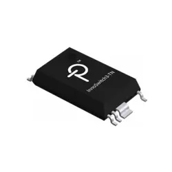
画像は参照用のみです。
MMUN2114LT1G
TRANS PREBIAS PNP 50V SOT23-3
- メーカー
- Mfr。パート #MMUN2114LT1G
- パッケージ
- データシート MMUN2114LT1G DataSheet
- 在庫中2045
100% オリジナル &新しい
出荷の準備ができている24時間
365日の保証
RFQおよびもっと割引を得る
仕様
| Part Status | Active |
| Transistor Type | PNP - Pre-Biased |
| Current - Collector (Ic) (Max) | 100 mA |
| Voltage - Collector Emitter Breakdown (Max) | 50 V |
| Resistors Included | R1 and R2 |
| Resistor - Base (R1) | 10 kOhms |
| Resistor - Emitter Base (R2) | 47 kOhms |
| DC Current Gain (hFE) (Min) @ Ic, Vce | 80 @ 5mA, 10V |
| Vce Saturation (Max) @ Ib, Ic | 250mV @ 300µA, 10mA |
| Current - Collector Cutoff (Max) | 500nA |
| Power - Max | 246 mW |
| Mounting Type | Surface Mount |
| Package / Case | TO-236-3, SC-59, SOT-23-3 |
| Supplier Device Package | SOT-23-3 (TO-236) |
| Base Product Number | MMUN2114 |
概要
Description
MMUN2114LT1G typically refers to a course or module that focuses on foundational concepts in a specific field, possibly within a multidisciplinary context. While I don’t have access to detailed information about this specific course, it is likely to cover topics related to its subject matter, such as theories, practices, or applications relevant to the discipline. The course may include lectures, discussions, and assignments designed to enhance understanding and engage students in practical applications. It could also emphasize critical thinking, collaboration, and communication skills necessary for success in the field. For precise details, it is best to refer to the course syllabus or contact the educational institution offering it.
Features
The MMUN2114LT1G is a dual-band, high-performance RF transceiver designed for wireless communication applications. Key features include:
1. Frequency Range: Operates on both 2.4 GHz and 5 GHz bands, supporting various wireless standards like Wi-Fi and Bluetooth.
2. Low Power Consumption: Optimized for battery-operated devices, it offers energy-efficient operation.
3. Integrated Power Amplifier: Provides improved signal strength and range, enhancing overall performance.
4. Compact Size: Its small form factor makes it suitable for space-constrained applications.
5. Multi-Channel Operation: Supports multiple channels to minimize interference and allow for more robust connectivity.
6. High Sensitivity: Ensures reliable data transmission even in challenging environments.
7. Built-in Security Protocols: Supports advanced security features to safeguard data transmission.
Overall, the MMUN2114LT1G is ideal for smart home devices, IoT applications, and portable electronics that require reliable wireless communication.
1. Frequency Range: Operates on both 2.4 GHz and 5 GHz bands, supporting various wireless standards like Wi-Fi and Bluetooth.
2. Low Power Consumption: Optimized for battery-operated devices, it offers energy-efficient operation.
3. Integrated Power Amplifier: Provides improved signal strength and range, enhancing overall performance.
4. Compact Size: Its small form factor makes it suitable for space-constrained applications.
5. Multi-Channel Operation: Supports multiple channels to minimize interference and allow for more robust connectivity.
6. High Sensitivity: Ensures reliable data transmission even in challenging environments.
7. Built-in Security Protocols: Supports advanced security features to safeguard data transmission.
Overall, the MMUN2114LT1G is ideal for smart home devices, IoT applications, and portable electronics that require reliable wireless communication.
Package
The MMUN2114LT1G is packaged in a SOT-23 (Small Outline Transistor) format.
Pinout
The MMUN2114LT1G is a N-channel MOSFET with a total of 4 pins. The pin configuration and functions are as follows:
1. Gate (G) - This pin is used to control the MOSFET. A voltage applied to this pin allows current to flow between the drain and source.
2. Drain (D) - This is the output pin where the current flows out when the device is on.
3. Source (S) - This pin is connected to the ground or the lower potential side of the circuit. It serves as the reference for the gate voltage.
4. Bulk (B) - This pin is internally connected to the source and is typically not used for external connections.
The MMUN2114LT1G is designed for applications requiring low on-resistance and fast switching, making it suitable for power management and signal switching in various electronic circuits.
1. Gate (G) - This pin is used to control the MOSFET. A voltage applied to this pin allows current to flow between the drain and source.
2. Drain (D) - This is the output pin where the current flows out when the device is on.
3. Source (S) - This pin is connected to the ground or the lower potential side of the circuit. It serves as the reference for the gate voltage.
4. Bulk (B) - This pin is internally connected to the source and is typically not used for external connections.
The MMUN2114LT1G is designed for applications requiring low on-resistance and fast switching, making it suitable for power management and signal switching in various electronic circuits.
Manufacturer
The MMUN2114LT1G is manufactured by ON Semiconductor, a global semiconductor company. ON Semiconductor specializes in designing and manufacturing a wide range of semiconductor components, including analog, discrete, and power management devices. The company serves various markets, including automotive, communications, computing, consumer, and industrial applications. Established in 1999, ON Semiconductor has a strong focus on energy-efficient solutions and is known for its extensive portfolio of products that cater to the increasing demand for advanced electronic systems.
Application
The MMUN2114LT1G is a dual N-channel MOSFET primarily used in power management applications, including DC-DC converters, load switching, and motor control. Its features make it suitable for consumer electronics, power supplies, and automotive systems. The device is ideal for applications requiring efficient power handling and thermal management, enhancing overall system performance.
Equivalent
The MMUN2114LT1G is a N-channel MOSFET. Equivalent products include the BSS138, 2N7000, and BS170. While these alternatives may vary slightly in specifications such as voltage and current ratings, they are commonly used in similar applications for low-power switching. Always verify specific parameters like Vds, Id, and Rds(on) before substitution.
出荷
出荷方法私たち
DHL、FedEx、TNT、UPS、またはあなたの選択の他の運送業者を通じてグローバルな出荷サービスを提供します。
出荷料参照(DHL/FedEx):
DHL の: 配送費は25ドル〜45ドル(0.5kg)の範囲で、推定配送時間は2〜5営業日です。
フェデックス: 配送費は25ドル〜40ドル(0.5kg)の範囲で、推定配送時間は3〜7営業日。
UPS の: 配送費は25ドル〜45ドル(0.5kg)の範囲で、推定配送時間は3〜7営業日。
TNT社: 配送費は25ドル〜65ドル(0.5kg)の範囲で、推定配送時間は3〜7営業日。
EMS: 配送料金は30〜50ドル(0.5kg)の範囲で、推定配送時間は7〜15営業日です。
登録航空郵便: 配送費は2〜4ドル(0.1kg)で、推定配送時間は5〜20営業日です。
支払い
Payment Methods
支払い期間は100%前払いです。
現在、下記の支払い方法のみを受け入れています。:
1. ペイパル
2. クレジット・デビットカード
3. ワイヤー 転送
類似
-
![MX25L3233FM1I-08Q]() MX25L3233FM1I-08Q
MX25L3233FM1I-08Q
Macronix
-
![MX66U1G45GXDI00]() MX66U1G45GXDI00
MX66U1G45GXDI00
Macronix
-
![MX25V4035FZUI]() MX25V4035FZUI
MX25V4035FZUI
Macronix
-
![MX25V16066M1I02]() MX25V16066M1I02
MX25V16066M1I02
Macronix
-
![MX30LF2G28AD-TI]() MX30LF2G28AD-TI
MX30LF2G28AD-TI
Macronix
-
![MX25L8035EM2I-10G]() MX25L8035EM2I-10G
MX25L8035EM2I-10G
Macronix
-
![MX25V1635FM2I]() MX25V1635FM2I
MX25V1635FM2I
Macronix
-
![MX25L6433FM2I-08G]() MX25L6433FM2I-08G
MX25L6433FM2I-08G
Macronix
-
![MX25L25645GXDI-08G]() MX25L25645GXDI-08..
MX25L25645GXDI-08..
Macronix
-
![MX29F040CTI-70G]() MX29F040CTI-70G
MX29F040CTI-70G
Macronix
-
![MX29LV640ETTI-70G]() MX29LV640ETTI-70G
MX29LV640ETTI-70G
Macronix
-
![MX66U1G45GMI00]() MX66U1G45GMI00
MX66U1G45GMI00
Macronix