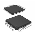
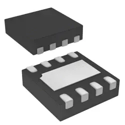
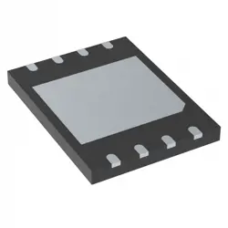
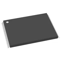
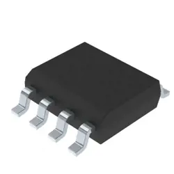
画像は参照用のみです。
MAX2601ESA
RF TRANS NPN 15V 1GHZ 8SOIC
- メーカー
- Mfr。パート #MAX2601ESA
- パッケージ 8-SOIC (0.154, 3.90mm Width) Exposed Pad
- データシート
- 在庫中603
100% オリジナル &新しい
出荷の準備ができている24時間
365日の保証
RFQおよびもっと割引を得る
仕様
| Supplier | Analog Devices Inc./Maxim Integrated,Rochester Electronics, LLC |
| Package | Tube,Tube |
| ProductStatus | Obsolete |
| TransistorType | NPN |
| Voltage-CollectorEmitterBreakdown(Max) | 15V |
| Frequency-Transition | 1GHz |
| NoiseFigure(dBTyp@f) | 3.3dB @ 836MHz |
| Gain | 11.6dB |
| Power-Max | 6.4W |
| DCCurrentGain(hFE)(Min)@IcVce | 100 @ 250mA, 3V |
| Current-Collector(Ic)(Max) | 1.2A |
| OperatingTemperature | 150°C (TJ) |
| MountingType | Surface Mount |
| Package/Case | 8-SOIC (0.154, 3.90mm Width) Exposed Pad |
概要
Description
MAX2601ESA is a Maxim Integrated (now Analog Devices) IC part number. The “ESA” suffix indicates a specific RoHS/packaging variant. The exact function of the MAX2601ESA device is defined by its datasheet, since the MAX26xx family covers diverse roles (analog/mixed-signal, RF front-end, clocking, etc.). An introductory read typically includes: what the IC does (its primary function), key features (voltage range, power, speed/bandwidth, performance metrics, integration), typical applications, pinout, recommended operating conditions, and package type.
Package
MAX2601ESA is in an 8-pin small-outline package (SOIC-8).
Pinout
Pin count: 16 pins (in the ESA package, RoHS-compliant).
Function: MAX2601ESA is a charge-pump DC-DC converter used to generate a negative supply (voltage inverter) from a positive input.
Function: MAX2601ESA is a charge-pump DC-DC converter used to generate a negative supply (voltage inverter) from a positive input.
Manufacturer
Manufacturer: Maxim Integrated (now part of Analog Devices).
What kind of company: a semiconductor company that designs and manufactures analog, mixed‑signal and RF integrated circuits (power management, interface, data converters, wireless/RF components) for communications, automotive, industrial and consumer markets.
What kind of company: a semiconductor company that designs and manufactures analog, mixed‑signal and RF integrated circuits (power management, interface, data converters, wireless/RF components) for communications, automotive, industrial and consumer markets.
Application
MAX2601ESA is used in RF wireless front‑end applications. Common areas include portable/mobile wireless devices (cell phones, GPS receivers, Bluetooth/Wi‑Fi modules), wireless sensor networks, automotive RF modules, and industrial radios. It supports front‑end blocks such as mixing/IF downconversion and PLL synthesis in transceivers, enabling compact, low‑power wireless links.
出荷
出荷方法私たち
DHL、FedEx、TNT、UPS、またはあなたの選択の他の運送業者を通じてグローバルな出荷サービスを提供します。
出荷料参照(DHL/FedEx):
DHL の: 配送費は25ドル〜45ドル(0.5kg)の範囲で、推定配送時間は2〜5営業日です。
フェデックス: 配送費は25ドル〜40ドル(0.5kg)の範囲で、推定配送時間は3〜7営業日。
UPS の: 配送費は25ドル〜45ドル(0.5kg)の範囲で、推定配送時間は3〜7営業日。
TNT社: 配送費は25ドル〜65ドル(0.5kg)の範囲で、推定配送時間は3〜7営業日。
EMS: 配送料金は30〜50ドル(0.5kg)の範囲で、推定配送時間は7〜15営業日です。
登録航空郵便: 配送費は2〜4ドル(0.1kg)で、推定配送時間は5〜20営業日です。
支払い
Payment Methods
支払い期間は100%前払いです。
現在、下記の支払い方法のみを受け入れています。:
1. ペイパル
2. クレジット・デビットカード
3. ワイヤー 転送
類似
-
![MX29F400CBTI-70G]() MX29F400CBTI-70G
Macronix
-
![MX25V5126FM1I]() MX25V5126FM1I
Macronix
-
![MX25V4035FZUI]() MX25V4035FZUI
Macronix
-
![MX30LF2G28AD-TI]() MX30LF2G28AD-TI
Macronix
-
![MX25L25673GMI-10G]() MX25L25673GMI-10G
Macronix
-
![MX25U51279GXDR00]() MX25U51279GXDR00
Macronix
-
![MX25U3232FZBI02]() MX25U3232FZBI02
Macronix
-
![MX25L12833FZ2I-10G]() MX25L12833FZ2I-10..
Macronix
-
![MX25L12835FZ2I-10G]() MX25L12835FZ2I-10..
Macronix
-
![MX29LV640ETTI-70G]() MX29LV640ETTI-70G
Macronix
-
![MX25L4006EM2I-12G]() MX25L4006EM2I-12G
Macronix
-
![MX25U3232FM2I02]() MX25U3232FM2I02
Macronix