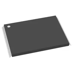
画像は参照用のみです。
MAX15068ATP+
IC HOT SWAP CTRLR GP 20TQFN
- メーカー
- Mfr。パート #MAX15068ATP+
- パッケージ WFQFN-20
- データシート
- 在庫中3792
100% オリジナル &新しい
出荷の準備ができている24時間
365日の保証
RFQおよびもっと割引を得る
仕様
| Package | Tray |
| ProductStatus | Active |
| Type | Hot Swap Controller, OR Controller |
| NumberofChannels | 1 |
| InternalSwitch(s) | No |
| Applications | General Purpose |
| Features | Auto Retry |
| ProgrammableFeatures | Circuit Breaker, Current Limit, Slew Rate, UVLO |
| Voltage-Supply | 3.7V ~ 18V |
| OperatingTemperature | -40°C ~ 125°C |
| Current-Supply | 4 mA |
| MountingType | Surface Mount |
| Package/Case | 20-WFQFN Exposed Pad |
概要
Description
The MAX15068ATP+ is a high-efficiency, step-down DC-DC converter designed by Maxim Integrated (now part of Analog Devices). It is intended for applications requiring compactness and reliability, such as industrial and automotive systems. This device can convert input voltages ranging from 4.5V to 60V to a lower DC output, providing up to 300mA of output current.
Key features of the MAX15068ATP+ include its wide input voltage range, high efficiency, and a low quiescent current, which is beneficial for battery-operated applications. The converter incorporates built-in protection features such as overcurrent protection, thermal shutdown, and input undervoltage lockout to enhance reliability and safety. Its compact TDFN (Thin Dual Flat No-Lead) package further supports space-constrained designs.
The device employs peak current-mode control architecture, which ensures good transient response and loop stability. It also supports a fixed-frequency operation, which helps minimize electromagnetic interference (EMI). These characteristics make the MAX15068ATP+ suitable for a wide range of applications, including power supply units, distributed power systems, and point-of-load regulation.
Features
The MAX15068ATP+ is a high-performance, versatile MOSFET driver IC designed for demanding applications. It features dual, high-speed, low-side MOSFET drivers capable of driving capacitive loads with peak currents up to 6A. The device operates with a wide input voltage range of 4.5V to 28V, making it suitable for a variety of power supply designs.
Key features include a low propagation delay of 12ns (typical), ensuring fast switching speeds critical for high-frequency applications. It also offers separate source and sink outputs, allowing independent control of rise and fall times, enhancing performance in different load conditions. The driver includes an enable pin for easier control of the output state and a robust UVLO (Undervoltage Lockout) feature to ensure reliable operation under low voltage conditions.
The MAX15068ATP+ is housed in a compact, thermally efficient 8-pin TDFN package, optimizing space in densely packed circuit designs. Its wide temperature range from -40°C to +125°C supports use in both consumer and industrial environments. Overall, the MAX15068ATP+ provides reliable, efficient, and flexible MOSFET driving capabilities, suitable for a wide array of power electronics applications.
Package
The MAX15068ATP+ is housed in a TQFN (Thin Quad Flat No-Lead) package. Specifically, it comes in a 16-pin TQFN package, which is compact and suitable for space-constrained applications.
Pinout
The MAX15068ATP+ is a high-voltage, high-side current-sense amplifier designed by Maxim Integrated. It comes in a small package with a specific pin configuration. The device is typically provided in a 6-pin TDFN package.
Here is a concise description of the pin functions:
1. IN+ (Pin 1): Non-inverting input for the differential voltage sensing.
2. IN- (Pin 2): Inverting input for the differential voltage sensing.
3. GND (Pin 3): Ground reference for the device.
4. OUT (Pin 4): Output voltage which is the amplified differential voltage across IN+ and IN-.
5. REF (Pin 5): Reference voltage input. The output voltage is referenced to this pin.
6. VCC (Pin 6): Supply voltage for the device.
These pin functions enable the MAX15068ATP+ to accurately sense currents by measuring the voltage across a shunt resistor, amplifying it, and outputting a proportional voltage, making it suitable for various power management applications.
Manufacturer
The MAX15068ATP+ is manufactured by Maxim Integrated, which is now part of Analog Devices, Inc. Analog Devices is a multinational semiconductor company that specializes in designing and manufacturing analog, mixed-signal, and digital signal processing (DSP) integrated circuits. The company serves a wide range of industries, including automotive, communications, consumer electronics, industrial, healthcare, and energy. Maxim Integrated, prior to its acquisition by Analog Devices, was known for its expertise in power management, interface, and microcontrollers, among other semiconductor solutions.
Application
The MAX15068ATP+ is a high-efficiency, step-down DC-DC converter. It is commonly used in applications requiring efficient power management, such as telecommunications equipment, industrial systems, and computing devices. Its ability to deliver high output current makes it suitable for powering microprocessors, FPGAs, and ASICs. Additionally, it can be used in battery-powered applications where energy efficiency is critical.
Equivalent
The MAX15068ATP+ is a high-voltage, high-side current-sense amplifier by Maxim Integrated. Equivalent products include the INA139 from Texas Instruments, the ZXCT1107 from Diodes Incorporated, and the LT1999 from Analog Devices. These alternatives offer similar high-voltage current-sense capabilities with varying specifications and performance characteristics. Always check the datasheets for detailed comparisons to ensure compatibility with your specific application.
出荷
出荷方法私たち
DHL、FedEx、TNT、UPS、またはあなたの選択の他の運送業者を通じてグローバルな出荷サービスを提供します。
出荷料参照(DHL/FedEx):
DHL の: 配送費は25ドル〜45ドル(0.5kg)の範囲で、推定配送時間は2〜5営業日です。
フェデックス: 配送費は25ドル〜40ドル(0.5kg)の範囲で、推定配送時間は3〜7営業日。
UPS の: 配送費は25ドル〜45ドル(0.5kg)の範囲で、推定配送時間は3〜7営業日。
TNT社: 配送費は25ドル〜65ドル(0.5kg)の範囲で、推定配送時間は3〜7営業日。
EMS: 配送料金は30〜50ドル(0.5kg)の範囲で、推定配送時間は7〜15営業日です。
登録航空郵便: 配送費は2〜4ドル(0.1kg)で、推定配送時間は5〜20営業日です。
支払い
Payment Methods
支払い期間は100%前払いです。
現在、下記の支払い方法のみを受け入れています。:
1. ペイパル
2. クレジット・デビットカード
3. ワイヤー 転送
類似
-
![MX25R8035FM1IL0]() MX25R8035FM1IL0
Macronix
-
![MX25V1635FZNQ03]() MX25V1635FZNQ03
Macronix
-
![MX29F400CBTI-70G]() MX29F400CBTI-70G
Macronix
-
![MX25V16066M2I02]() MX25V16066M2I02
Macronix
-
![MX25L8035EM2I-10G]() MX25L8035EM2I-10G
Macronix
-
![MX25L25673GMI-08G]() MX25L25673GMI-08G
Macronix
-
![MX29GL512FHXFI-11G]() MX29GL512FHXFI-11..
Macronix
-
![MX25L6433FM2I-08G]() MX25L6433FM2I-08G
Macronix
-
![MX25U6435FM2I-10G]() MX25U6435FM2I-10G
Macronix
-
![MX25L12833FZ2I-10G]() MX25L12833FZ2I-10..
Macronix
-
![MX25L12833FZNI-10G]() MX25L12833FZNI-10..
Macronix
-
![MX29LV160DTTI-70G]() MX29LV160DTTI-70G
Macronix