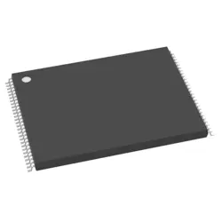
画像は参照用のみです。
LTC2050CS5
- メーカー
- Mfr。パート #LTC2050CS5
- パッケージ
- データシート LTC2050CS5 DataSheet
- 在庫中5718
100% オリジナル &新しい
出荷の準備ができている24時間
365日の保証
RFQおよびもっと割引を得る
仕様
| Operating Supply Current | 800 uA |
| Mounting Style | SMD/SMT |
| Minimum Operating Temperature | 0 C |
| Maximum Operating Temperature | + 70 C |
| Series | LTC2050 |
| Brand | Analog Devices |
| Number of Channels | 1 Channel |
| Product Type | Precision Amplifiers |
| Subcategory | Amplifier ICs |
| Shipping Restrictions | Mouser does not presently sell this product in your region. |
| Package / Case | SOT-5 |
| Supply Voltage - Min | 2.7 V |
| Supply Voltage - Max | 6 V |
| Vos - Input Offset Voltage | 500 nV |
| Product | Operational Amplifiers |
| GBP - Gain Bandwidth Product | 3 MHz |
| SR - Slew Rate | 2 V/us |
| CMRR - Common Mode Rejection Ratio | 90 dB |
| Output Current per Channel | 10 mA |
| Ib - Input Bias Current | 20 pA |
| In - Input Noise Current Density | 0.003 pA/sqrt Hz |
| PSRR - Power Supply Rejection Ratio | 130 dB |
| Shutdown | No Shutdown |
| Ios - Input Offset Current | 200 pA |
| Height | 1 mm |
| Voltage Gain dB | 140 dB |
| Output Type | Rail-to-Rail |
概要
Description
The LTC2050CS5 is a precision, zero-drift operational amplifier designed by Linear Technology, now part of Analog Devices. It is notable for its extremely low offset voltage and low frequency noise, making it ideal for high-precision applications. The amplifier operates with a supply voltage range from 2.7V to 6V, allowing for flexibility in various low-voltage applications.
One of its key features is the chopper-stabilized architecture, which helps maintain performance consistency over time and temperature. This architecture effectively eliminates offset voltage drift, providing stable and accurate output even in challenging conditions. The LTC2050CS5 is available in a compact SOT-23 package, making it suitable for space-constrained designs.
Typical applications for the LTC2050CS5 include sensor interfacing, precision data acquisition systems, and medical instrumentation where low noise and high accuracy are critical. Additionally, its low input bias current and high common-mode rejection ratio (CMRR) further enhance its suitability for precision applications. Overall, the LTC2050CS5 is a robust choice for designers looking to implement high-performance amplification in their circuits.
Features
The LTC2050CS5 is a precision operational amplifier from Analog Devices, designed for applications requiring low power and high accuracy. Key features include:
1. Low Offset Voltage: It has a very low input offset voltage, typically around 3 µV, which ensures high precision in signal processing.
2. Low Noise: The amplifier is characterized by low input noise, making it suitable for applications demanding high signal fidelity.
3. Low Power Consumption: It operates at low power, drawing minimal supply current, which is ideal for battery-operated devices.
4. Rail-to-Rail Output: The LTC2050CS5 provides a rail-to-rail output stage, maximizing the dynamic range and flexibility in various applications.
5. Wide Supply Range: It operates over a wide supply voltage range, enhancing its versatility in different systems.
6. Temperature Stability: The device exhibits excellent temperature stability, maintaining performance over a wide range of operating conditions.
These features make the LTC2050CS5 suitable for precision instrumentation, medical devices, and portable electronic applications where accuracy and low power are critical.
Package
The LTC2050CS5 is a precision operational amplifier that is available in the SOT-23 package type. The SOT-23 package is a small, surface-mount technology package commonly used for electronic components.
Pinout
The LTC2050CS5 is a precision operational amplifier with a pin count of 5. It is designed for applications that require low power consumption and high precision. The primary functions of the LTC2050CS5 include zero-drift, low offset voltage, and low noise operation, making it suitable for precision signal conditioning. The typical pin configuration for the LTC2050CS5 in a SOT-23 package includes:
1. V+ (Positive Supply Voltage): Powers the operational amplifier.
2. V- (Negative Supply Voltage or Ground): Completes the power supply circuit.
3. Non-Inverting Input (Vin+): Accepts the input signal that is to be amplified.
4. Inverting Input (Vin-): Accepts the input signal for differential amplification.
5. Output (Vout): Provides the amplified signal.
This operational amplifier is often used in applications like sensor interfacing and precision data acquisition systems due to its accuracy and reliability.
Manufacturer
The LTC2050CS5 is manufactured by Analog Devices, Inc. Analog Devices is a multinational semiconductor company known for designing and manufacturing a broad range of analog, mixed-signal, and digital signal processing (DSP) integrated circuits. These components are used in various electronic equipment, including industrial, automotive, communications, and consumer electronics. The company is recognized for its expertise in high-performance analog technology and its focus on innovation in sensing, measuring, and interpreting real-world phenomena.
Application
The LTC2050CS5 is a precision zero-drift operational amplifier. Its application areas include sensor signal conditioning, precision data acquisition systems, instrumentation amplifiers, low-frequency active filters, and medical instrumentation. It is particularly well-suited for applications requiring high accuracy and low offset voltage, such as strain gauge amplifiers, thermocouple amplifiers, and other analog circuits where drift and noise must be minimized.
Equivalent
The LTC2050CS5 is a precision zero-drift operational amplifier. Equivalent products include:
1. AD8538 by Analog Devices
2. MCP6V01 by Microchip Technology
3. OPA333 by Texas Instruments
These alternatives offer similar low offset voltage, low drift, and low noise performance suitable for precision applications. Always check the specific datasheets to ensure compatibility with your application's requirements.
出荷
出荷方法私たち
DHL、FedEx、TNT、UPS、またはあなたの選択の他の運送業者を通じてグローバルな出荷サービスを提供します。
出荷料参照(DHL/FedEx):
DHL の: 配送費は25ドル〜45ドル(0.5kg)の範囲で、推定配送時間は2〜5営業日です。
フェデックス: 配送費は25ドル〜40ドル(0.5kg)の範囲で、推定配送時間は3〜7営業日。
UPS の: 配送費は25ドル〜45ドル(0.5kg)の範囲で、推定配送時間は3〜7営業日。
TNT社: 配送費は25ドル〜65ドル(0.5kg)の範囲で、推定配送時間は3〜7営業日。
EMS: 配送料金は30〜50ドル(0.5kg)の範囲で、推定配送時間は7〜15営業日です。
登録航空郵便: 配送費は2〜4ドル(0.1kg)で、推定配送時間は5〜20営業日です。
支払い
Payment Methods
支払い期間は100%前払いです。
現在、下記の支払い方法のみを受け入れています。:
1. ペイパル
2. クレジット・デビットカード
3. ワイヤー 転送
類似
-
![MX25L3233FZBI-08Q]() MX25L3233FZBI-08Q
Macronix
-
![MX25L3233FM1I-08Q]() MX25L3233FM1I-08Q
Macronix
-
![MX25V1635FZNI]() MX25V1635FZNI
Macronix
-
![MX25V5126FM1I]() MX25V5126FM1I
Macronix
-
![MX25V2033FM1I]() MX25V2033FM1I
Macronix
-
![MX25V16066M1I02]() MX25V16066M1I02
Macronix
-
![MX30LF2G28AD-TI]() MX30LF2G28AD-TI
Macronix
-
![MX25L6433FM2I-08G]() MX25L6433FM2I-08G
Macronix
-
![MX25L12833FZNI-10G]() MX25L12833FZNI-10..
Macronix
-
![MX25L12835FZ2I-10G]() MX25L12835FZ2I-10..
Macronix
-
![MX29F800CBTI-70G]() MX29F800CBTI-70G
Macronix
-
![MX29LV640ETTI-70G]() MX29LV640ETTI-70G
Macronix