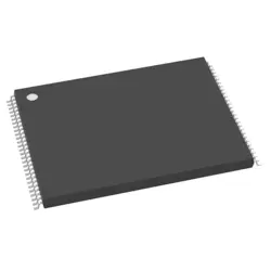
画像は参照用のみです。
LTC1597ACG
Digital to Analog Converters - DAC LTC1597 - 16-Bit Parallel Low Glitch Multiplying DAC with 4-Quadrant Resistors
- メーカー
- Mfr。パート #LTC1597ACG
- パッケージ
- データシート LTC1597ACG DataSheet
- 在庫中18206
100% オリジナル &新しい
出荷の準備ができている24時間
365日の保証
RFQおよびもっと割引を得る
仕様
概要
Description
Key features include low power consumption (approximately 30 mW), differential input for improved noise performance, and a wide operating temperature range. The LTC1597ACG also includes built-in sample-and-hold circuitry, which aids in capturing fast-changing signals accurately. Its compact 28-lead SSOP package allows for space-efficient designs in various applications, including portable instrumentation and industrial automation. Overall, the LTC1597ACG is an excellent choice for engineers seeking a high-performance ADC for demanding applications.
Features
1. Speed: It operates at a maximum conversion rate of 1 MSPS (million samples per second).
2. Resolution: Offers 12-bit resolution, providing a high level of detail in signal conversion.
3. Input Voltage Range: It supports a single-ended input voltage range of 0V to 5V.
4. Low Power: Consumes only 15 mW in normal operation, making it suitable for battery-powered devices.
5. Differential Inputs: Can accept differential input signals to reduce noise.
6. Built-In Sample-and-Hold: Features an integrated sample-and-hold circuit for improved signal accuracy.
7. Serial Interface: Communicates via a serial interface for easy integration with microcontrollers and digital processors.
8. Temperature Range: Operates effectively over an extended temperature range, enhancing reliability in various environments.
These features make the LTC1597ACG ideal for applications in instrumentation, audio processing, and other high-speed data acquisition systems.
Package
Pinout
### Pin Functions:
1. VDD: Power supply.
2. VSS: Ground reference.
3. REF: Reference voltage input for the ADC.
4. AIN: Analog input for conversion.
5. BUSY: Indicates when the ADC is converting.
6. CS: Chip select for enabling the device.
7. RD: Read strobe signal for data output.
8. WR: Write strobe for initiating the conversion.
9. CLK: Clock input for timing control.
10. D0-D7: Data output lines (8 bits).
11. AGND: Analog ground.
12. SYNC: Synchronization input for multiple ADCs.
The LTC1597ACG is designed for applications requiring precise analog signal conversion, typically in measurement and control systems.
Manufacturer
Application
Equivalent
出荷
出荷方法私たち
DHL、FedEx、TNT、UPS、またはあなたの選択の他の運送業者を通じてグローバルな出荷サービスを提供します。
出荷料参照(DHL/FedEx):
DHL の: 配送費は25ドル〜45ドル(0.5kg)の範囲で、推定配送時間は2〜5営業日です。
フェデックス: 配送費は25ドル〜40ドル(0.5kg)の範囲で、推定配送時間は3〜7営業日。
UPS の: 配送費は25ドル〜45ドル(0.5kg)の範囲で、推定配送時間は3〜7営業日。
TNT社: 配送費は25ドル〜65ドル(0.5kg)の範囲で、推定配送時間は3〜7営業日。
EMS: 配送料金は30〜50ドル(0.5kg)の範囲で、推定配送時間は7〜15営業日です。
登録航空郵便: 配送費は2〜4ドル(0.1kg)で、推定配送時間は5〜20営業日です。
支払い
Payment Methods
支払い期間は100%前払いです。
現在、下記の支払い方法のみを受け入れています。:
1. ペイパル
2. クレジット・デビットカード
3. ワイヤー 転送
類似
-
![MX25L3233FZBI-08Q]() MX25L3233FZBI-08Q
Macronix
-
![MX25V1635FZNI]() MX25V1635FZNI
Macronix
-
![MX29F400CBTI-70G]() MX29F400CBTI-70G
Macronix
-
![MX66U1G45GXDI00]() MX66U1G45GXDI00
Macronix
-
![MX25V4035FZUI]() MX25V4035FZUI
Macronix
-
![MX25V2033FM1I]() MX25V2033FM1I
Macronix
-
![MX25R3235FZNIL0]() MX25R3235FZNIL0
Macronix
-
![MX30LF2G28AD-TI]() MX30LF2G28AD-TI
Macronix
-
![MX25U6435FM2I-10G]() MX25U6435FM2I-10G
Macronix
-
![MX25L12833FM2I-10G]() MX25L12833FM2I-10..
Macronix
-
![MX25L12833FZNI-10G]() MX25L12833FZNI-10..
Macronix
-
![MX29LV160DTTI-70G]() MX29LV160DTTI-70G
Macronix