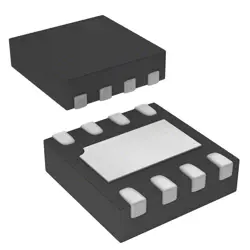
画像は参照用のみです。
LTC1261CS8-4
Switching Voltage Regulators LTC1261 - Switched Capacitor Regulated Voltage Inverter
- メーカー
- Mfr。パート #LTC1261CS8-4
- パッケージ
- データシート LTC1261CS8-4 DataSheet
- 在庫中25486
100% オリジナル &新しい
出荷の準備ができている24時間
365日の保証
RFQおよびもっと割引を得る
仕様
概要
Description
Key features include an internal reference voltage, programmable gain, and a parallel output format, which allows easy interfacing with microcontrollers and digital signal processors. The LTC1261 also incorporates built-in sample-and-hold capabilities, ensuring accurate readings of rapidly changing signals.
The chip is offered in an 8-pin SOIC package, making it compact for space-constrained designs. Overall, the LTC1261CS8-4 is ideal for applications requiring reliable and high-speed data conversion in low-power environments.
Features
1. Conversion Speed: Up to 100 kSamples/s, allowing for rapid data acquisition.
2. Low Power Consumption: Operates with a supply voltage of 5V and consumes as little as 70 mW, making it suitable for battery-powered devices.
3. Single Supply Operation: Simplifies the design by allowing operation from a single power source.
4. Differential Input: Supports differential input signals, providing increased noise immunity and improved performance in noisy environments.
5. Internal Reference: Comes with an internal 2.5V reference voltage, which can be bypassed for external references if needed.
6. Serial Interface: Features a serial output interface for easy communication with microcontrollers or DSPs.
7. Programmable Gain Amplifier: Allows for adjustable gain settings to accommodate a variety of input signal ranges.
These features make the LTC1261CS8-4 ideal for applications in data acquisition, instrumentation, and portable measurement devices.
Package
Pinout
Pin Count: 8 pins
Function of Pins:
1. V+ (Pin 1): Positive supply voltage.
2. V- (Pin 2): Negative supply voltage.
3. AIN (Pin 3): Analog input for the signal to be converted.
4. AGND (Pin 4): Analog ground reference.
5. D0-D3 (Pins 5-8): Digital output pins representing the 12-bit converted data (D0 is the least significant bit).
The LTC1261 is designed for applications requiring fast data conversion, such as in signal processing and instrumentation, with features that ensure accuracy and efficiency.
Manufacturer
Application
Equivalent
出荷
出荷方法私たち
DHL、FedEx、TNT、UPS、またはあなたの選択の他の運送業者を通じてグローバルな出荷サービスを提供します。
出荷料参照(DHL/FedEx):
DHL の: 配送費は25ドル〜45ドル(0.5kg)の範囲で、推定配送時間は2〜5営業日です。
フェデックス: 配送費は25ドル〜40ドル(0.5kg)の範囲で、推定配送時間は3〜7営業日。
UPS の: 配送費は25ドル〜45ドル(0.5kg)の範囲で、推定配送時間は3〜7営業日。
TNT社: 配送費は25ドル〜65ドル(0.5kg)の範囲で、推定配送時間は3〜7営業日。
EMS: 配送料金は30〜50ドル(0.5kg)の範囲で、推定配送時間は7〜15営業日です。
登録航空郵便: 配送費は2〜4ドル(0.1kg)で、推定配送時間は5〜20営業日です。
支払い
Payment Methods
支払い期間は100%前払いです。
現在、下記の支払い方法のみを受け入れています。:
1. ペイパル
2. クレジット・デビットカード
3. ワイヤー 転送
類似
-
![MX25V1635FZNI]() MX25V1635FZNI
Macronix
-
![MX66U1G45GXDI00]() MX66U1G45GXDI00
Macronix
-
![MX25V2033FM1I]() MX25V2033FM1I
Macronix
-
![MX30LF2G28AD-TI]() MX30LF2G28AD-TI
Macronix
-
![MX25L8035EM2I-10G]() MX25L8035EM2I-10G
Macronix
-
![MX25U25643GZNI00]() MX25U25643GZNI00
Macronix
-
![MX25R1635FZUIH0]() MX25R1635FZUIH0
Macronix
-
![MX25L6433FM2I-08G]() MX25L6433FM2I-08G
Macronix
-
![MX25U6435FM2I-10G]() MX25U6435FM2I-10G
Macronix
-
![MX25L12833FM2I-10G]() MX25L12833FM2I-10..
Macronix
-
![MX25L12833FZ2I-10G]() MX25L12833FZ2I-10..
Macronix
-
![MX25L12833FZNI-10G]() MX25L12833FZNI-10..
Macronix