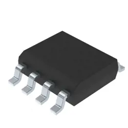
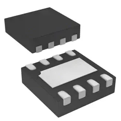
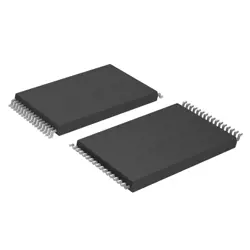
画像は参照用のみです。
LT8636JV#WTRPBF
Switching Voltage Regulators 42V, 5A/7A Peak Synchronous Step-Down Silent Switcher with 2.5?A Quiescent Current
- メーカー
- Mfr。パート #LT8636JV#WTRPBF
- パッケージ
- データシート LT8636JV#WTRPBF DataSheet
- 在庫中17184
100% オリジナル &新しい
出荷の準備ができている24時間
365日の保証
RFQおよびもっと割引を得る
仕様
概要
Description
Key features include a high switching frequency, which allows for smaller external components, and an adjustable output voltage down to 0.8V. It also incorporates various protection mechanisms such as thermal shutdown and overcurrent protection. The LT8636 operates in a burst mode to improve efficiency at light loads, further enhancing its applicability in battery-powered devices.
The package type (JV) is a thermally enhanced 4mm x 4mm QFN, allowing for efficient heat dissipation. Overall, the LT8636JV#WTRPBF is ideal for applications like portable equipment, industrial automation, and RF systems where low noise and compact design are critical.
Features
1. Output Current: Supports up to 2A continuous output current.
2. Efficiency: Achieves high efficiency (up to 95%) across a broad load range.
3. Low Quiescent Current: Operates with low quiescent current (typically 10µA), making it suitable for battery-powered applications.
4. Switching Frequency: Fixed and adjustable switching frequencies (up to 2MHz) offer design flexibility.
5. Soft-Start: Integrated soft-start function helps prevent inrush current during startup.
6. Thermal Protection: Features built-in thermal protection to prevent overheating.
7. Compact Package: Available in a 3mm x 3mm DFN package, ideal for space-constrained designs.
This device is well-suited for a variety of applications, including portable devices, automotive electronics, and industrial systems, where efficiency and compact design are critical.
Package
Pinout
1. VIN (Pin 1): Input voltage.
2. GND (Pin 2): Ground connection.
3. SW (Pin 3): Switch node for the internal PMOS transistor.
4. VOUT (Pin 4): Output voltage.
5. COMP (Pin 5): Compensation node for stability.
6. SS (Pin 6): Soft-start pin for controlling the startup time.
7. FB (Pin 7): Feedback pin for setting the output voltage.
8. EN (Pin 8): Enable pin for turning the device on/off.
9. PG (Pin 9): Power good indicator.
10. VC (Pin 10): Voltage control pin for loop compensation.
This LDO is designed to provide a stable output with low noise and high accuracy for various applications.
Manufacturer
Application
Equivalent
出荷
出荷方法私たち
DHL、FedEx、TNT、UPS、またはあなたの選択の他の運送業者を通じてグローバルな出荷サービスを提供します。
出荷料参照(DHL/FedEx):
DHL の: 配送費は25ドル〜45ドル(0.5kg)の範囲で、推定配送時間は2〜5営業日です。
フェデックス: 配送費は25ドル〜40ドル(0.5kg)の範囲で、推定配送時間は3〜7営業日。
UPS の: 配送費は25ドル〜45ドル(0.5kg)の範囲で、推定配送時間は3〜7営業日。
TNT社: 配送費は25ドル〜65ドル(0.5kg)の範囲で、推定配送時間は3〜7営業日。
EMS: 配送料金は30〜50ドル(0.5kg)の範囲で、推定配送時間は7〜15営業日です。
登録航空郵便: 配送費は2〜4ドル(0.1kg)で、推定配送時間は5〜20営業日です。
支払い
Payment Methods
支払い期間は100%前払いです。
現在、下記の支払い方法のみを受け入れています。:
1. ペイパル
2. クレジット・デビットカード
3. ワイヤー 転送
類似
-
![MX25V1635FZNI]() MX25V1635FZNI
Macronix
-
![MX25V16066M2I02]() MX25V16066M2I02
Macronix
-
![MX25R6435FBDIL0]() MX25R6435FBDIL0
Macronix
-
![MX25L25673GMI-08G]() MX25L25673GMI-08G
Macronix
-
![MX29GL512FHXFI-11G]() MX29GL512FHXFI-11..
Macronix
-
![MX25L2006EM1I-12G]() MX25L2006EM1I-12G
Macronix
-
![MX25V1635FM2I]() MX25V1635FM2I
Macronix
-
![MX25U3232FZBI02]() MX25U3232FZBI02
Macronix
-
![MX25L6433FM2I-08G]() MX25L6433FM2I-08G
Macronix
-
![MX25U25645GXDI00]() MX25U25645GXDI00
Macronix
-
![MX25L25645GXDI-08G]() MX25L25645GXDI-08..
Macronix
-
![MX29F040CTI-70G]() MX29F040CTI-70G
Macronix