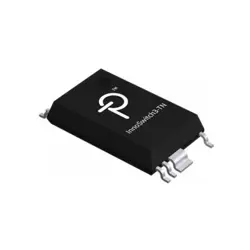
画像は参照用のみです。
LT1054IDWR
IC REG CHARG PUMP INV 16SOIC
- メーカー
- Mfr。パート #LT1054IDWR
- パッケージ SOIC (DW)-16
- データシート
- 在庫中6049
100% オリジナル &新しい
出荷の準備ができている24時間
365日の保証
RFQおよびもっと割引を得る
仕様
| Package | Tape & Reel (TR),Cut Tape (CT),Bulk |
| ProductStatus | Active |
| Function | Ratiometric, Step-Up |
| OutputConfiguration | Positive or Negative |
| Topology | Charge Pump |
| OutputType | Adjustable (Fixed) |
| NumberofOutputs | 1 |
| Voltage-Input(Min) | 3.5V |
| Voltage-Input(Max) | 15V |
| Voltage-Output(Min/Fixed) | 3.5V (-Vin, 2Vin) |
| Voltage-Output(Max) | 26.4V |
| Current-Output | 100mA |
| Frequency-Switching | 25kHz |
| SynchronousRectifier | No |
| OperatingTemperature | -40°C ~ 85°C (TA) |
| MountingType | Surface Mount |
| Package/Case | 16-SOIC (0.295, 7.50mm Width) |
概要
Description
The LT1054IDWR is a versatile voltage converter integrated circuit (IC) manufactured by Texas Instruments. This device is widely used for power supply applications, as it can efficiently convert voltage levels in various configurations. It combines the functions of a DC-DC converter with a voltage regulator, making it suitable for generating positive and negative voltages from a single input supply.
Key features of the LT1054IDWR include low quiescent current, high-efficiency charge pump operation, and the ability to deliver relatively high output current. It supports both step-up (boost) and step-down (buck) voltage conversion and can be configured for inverting voltage applications as well. This makes it particularly useful in systems where dual power supply voltages are required or where the input voltage is not stable.
The package type, IDWR, indicates a specific variant in terms of size and thermal performance, often suited for surface-mount applications. The LT1054IDWR is typically used in battery-powered devices, portable instruments, and other electronic applications that require efficient power management in a compact form factor.
Key features of the LT1054IDWR include low quiescent current, high-efficiency charge pump operation, and the ability to deliver relatively high output current. It supports both step-up (boost) and step-down (buck) voltage conversion and can be configured for inverting voltage applications as well. This makes it particularly useful in systems where dual power supply voltages are required or where the input voltage is not stable.
The package type, IDWR, indicates a specific variant in terms of size and thermal performance, often suited for surface-mount applications. The LT1054IDWR is typically used in battery-powered devices, portable instruments, and other electronic applications that require efficient power management in a compact form factor.
Features
The LT1054IDWR is a versatile switched-capacitor voltage converter IC. Key features include:
1. Input Voltage Range: Typically operates within 3.5V to 15V, allowing flexibility for various applications.
2. Output Voltage: Capable of inverting or doubling the input voltage, useful for generating negative voltages from positive input or increasing voltage levels.
3. Efficiency: High efficiency due to low quiescent current and internal oscillator.
4. Current Output: Provides up to 100mA output current, suitable for low-power applications.
5. Frequency: Operates with a nominal switching frequency of around 25kHz.
6. Temperature Range: Industrial temperature range operation from -40°C to 85°C, suitable for harsh environments.
7. Protection: Includes features like short-circuit protection and thermal shutdown for enhanced reliability.
8. Package: Available in a surface-mount package, making it suitable for compact circuit designs.
9. Adjustable Output: Allows output voltage to be set using external components for customized applications.
10. Low External Component Count: Simplifies design and reduces the overall size and cost of the solution.
The LT1054IDWR is widely used in applications requiring efficient voltage conversion with minimal external components.
1. Input Voltage Range: Typically operates within 3.5V to 15V, allowing flexibility for various applications.
2. Output Voltage: Capable of inverting or doubling the input voltage, useful for generating negative voltages from positive input or increasing voltage levels.
3. Efficiency: High efficiency due to low quiescent current and internal oscillator.
4. Current Output: Provides up to 100mA output current, suitable for low-power applications.
5. Frequency: Operates with a nominal switching frequency of around 25kHz.
6. Temperature Range: Industrial temperature range operation from -40°C to 85°C, suitable for harsh environments.
7. Protection: Includes features like short-circuit protection and thermal shutdown for enhanced reliability.
8. Package: Available in a surface-mount package, making it suitable for compact circuit designs.
9. Adjustable Output: Allows output voltage to be set using external components for customized applications.
10. Low External Component Count: Simplifies design and reduces the overall size and cost of the solution.
The LT1054IDWR is widely used in applications requiring efficient voltage conversion with minimal external components.
Package
The LT1054IDWR is a voltage converter IC packaged in a surface-mount SOIC (Small Outline Integrated Circuit) package type. Specifically, it comes in a 16-pin SOIC wide-body package, which is denoted by the "DW" in its part number.
Pinout
The LT1054IDWR is a switched-capacitor voltage converter integrated circuit (IC) manufactured by Texas Instruments. It is typically used for voltage inversion, doubling, or regulation. The device comes in a 14-pin SOIC (Small Outline Integrated Circuit) package.
Here's a brief overview of its pin functions:
1. CAP+: Positive terminal of the charge-pump capacitor.
2. CAP-: Negative terminal of the charge-pump capacitor.
3. GND: Ground connection.
4. VOUT: Output voltage.
5. VIN: Input voltage.
6. S: Shutdown pin; used to enable or disable the device.
7. FB/ADJ: Feedback/adjust pin used for voltage regulation.
8. SW1 and SW2: Internal switches associated with charge-pump operation.
9. VREF: Reference voltage output.
10. D1 - D4: Diode connections for the charge-pump circuit.
The LT1054IDWR is designed for applications requiring efficient voltage conversion with minimal external components, making it suitable for battery-powered devices and other compact electronic applications.
Here's a brief overview of its pin functions:
1. CAP+: Positive terminal of the charge-pump capacitor.
2. CAP-: Negative terminal of the charge-pump capacitor.
3. GND: Ground connection.
4. VOUT: Output voltage.
5. VIN: Input voltage.
6. S: Shutdown pin; used to enable or disable the device.
7. FB/ADJ: Feedback/adjust pin used for voltage regulation.
8. SW1 and SW2: Internal switches associated with charge-pump operation.
9. VREF: Reference voltage output.
10. D1 - D4: Diode connections for the charge-pump circuit.
The LT1054IDWR is designed for applications requiring efficient voltage conversion with minimal external components, making it suitable for battery-powered devices and other compact electronic applications.
Manufacturer
The LT1054IDWR is manufactured by Texas Instruments. Texas Instruments is a technology company that designs and manufactures semiconductors and various integrated circuits, which are used in a wide range of electronic applications. They serve industries such as automotive, industrial, personal electronics, communications equipment, and enterprise systems.
Application
The LT1054IDWR is a versatile charge pump DC-DC converter commonly used for voltage conversion applications. Key areas include generating negative voltage for operational amplifiers, powering sensors, biasing LCD displays, and providing isolated power supply rails in mixed-signal or data acquisition systems. It is also used in battery-powered devices for efficient power management and in applications requiring voltage inversion or doubling.
Equivalent
The LT1054IDWR is a switched-capacitor voltage converter/inverter. Equivalent products include the LM2662, MAX1044, and ICL7660. These components perform similar functions, typically used for voltage inversion or doubling in power supply designs. Always verify specifications like voltage range, frequency, and current capability to ensure compatibility with your specific application.
出荷
出荷方法私たち
DHL、FedEx、TNT、UPS、またはあなたの選択の他の運送業者を通じてグローバルな出荷サービスを提供します。
出荷料参照(DHL/FedEx):
DHL の: 配送費は25ドル〜45ドル(0.5kg)の範囲で、推定配送時間は2〜5営業日です。
フェデックス: 配送費は25ドル〜40ドル(0.5kg)の範囲で、推定配送時間は3〜7営業日。
UPS の: 配送費は25ドル〜45ドル(0.5kg)の範囲で、推定配送時間は3〜7営業日。
TNT社: 配送費は25ドル〜65ドル(0.5kg)の範囲で、推定配送時間は3〜7営業日。
EMS: 配送料金は30〜50ドル(0.5kg)の範囲で、推定配送時間は7〜15営業日です。
登録航空郵便: 配送費は2〜4ドル(0.1kg)で、推定配送時間は5〜20営業日です。
支払い
Payment Methods
支払い期間は100%前払いです。
現在、下記の支払い方法のみを受け入れています。:
1. ペイパル
2. クレジット・デビットカード
3. ワイヤー 転送
類似
-
![MX25V1635FZNQ03]() MX25V1635FZNQ03
MX25V1635FZNQ03
Macronix
-
![MX25V4035FZUI]() MX25V4035FZUI
MX25V4035FZUI
Macronix
-
![MX25V16066M1I02]() MX25V16066M1I02
MX25V16066M1I02
Macronix
-
![MX30LF2G28AD-TI]() MX30LF2G28AD-TI
MX30LF2G28AD-TI
Macronix
-
![MX25L8035EM2I-10G]() MX25L8035EM2I-10G
MX25L8035EM2I-10G
Macronix
-
![MX25U51279GXDR00]() MX25U51279GXDR00
MX25U51279GXDR00
Macronix
-
![MX25L12833FM2I-10G]() MX25L12833FM2I-10..
MX25L12833FM2I-10..
Macronix
-
![MX25L12833FZNI-10G]() MX25L12833FZNI-10..
MX25L12833FZNI-10..
Macronix
-
![MX25L12835FZ2I-10G]() MX25L12835FZ2I-10..
MX25L12835FZ2I-10..
Macronix
-
![MX25L25645GXDI-08G]() MX25L25645GXDI-08..
MX25L25645GXDI-08..
Macronix
-
![MX29F040CTI-70G]() MX29F040CTI-70G
MX29F040CTI-70G
Macronix
-
![MX66U1G45GMI00]() MX66U1G45GMI00
MX66U1G45GMI00
Macronix