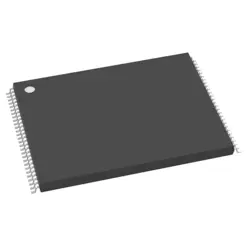
画像は参照用のみです。
LPC1114FBD48/302
ARM Microcontrollers - MCU LPC1114FBD48/LQFP48//302/STANDARD MARKING * TRAY P
- メーカー
- Mfr。パート #LPC1114FBD48/302
- パッケージ
- データシート LPC1114FBD48/302 DataSheet
- 在庫中9341
100% オリジナル &新しい
出荷の準備ができている24時間
365日の保証
RFQおよびもっと割引を得る
仕様
概要
Description
The LPC1114FBD48/302 is a microcontroller from NXP Semiconductors, part of the LPC1100 series. It features a 32-bit ARM Cortex-M0 core, operating at speeds up to 50 MHz, with a single-cycle architecture that provides efficient performance for embedded applications. The device includes 32 KB of flash memory and 8 KB of SRAM, making it suitable for various applications, including consumer electronics and industrial control.
Key features include multiple I/O ports, a range of peripherals such as UART, SPI, I2C, and a 10-bit ADC. The LPC1114FBD48/302 supports low-power modes, enhancing battery life in portable devices. Its small footprint (48-pin LQFP package) allows for space-efficient designs.
Development is facilitated by various IDEs and toolchains, including NXP's own LPCXpresso and Keil MDK. The microcontroller's combination of performance, integrated features, and power efficiency makes it a versatile choice for numerous embedded system applications.
Features
The LPC1114FBD48/302 is a microcontroller from NXP's LPC1100 series. Key features include:
- Core: ARM Cortex-M0 processor running at up to 50 MHz.
- Flash Memory: 32 KB of on-chip flash memory.
- RAM: 8 KB of SRAM.
- I/O Ports: Up to 24 GPIO pins with configurable functions.
- Timers: Multiple 32-bit timers for various timing applications.
- ADC: 10-bit ADC with up to 8 channels.
- Communication Interfaces:
- I2C, UART, and SPI for versatile connectivity options.
- Power Management: Low power modes for energy-efficient operation.
- Interrupts: Nested Vectored Interrupt Controller (NVIC) for efficient interrupt handling.
- Operating Voltage: 2.4V to 3.6V.
- Package: Available in a compact 48-pin LQFP package.
This microcontroller is suitable for various applications, including automotive, industrial control, and consumer electronics, due to its balance of performance and power efficiency.
Package
The LPC1114FBD48/302 is packaged in a 48-pin LQFP (Low Profile Quad Flat Package). This surface-mount package features a 7mm x 7mm footprint, ideal for compact designs requiring space efficiency.
Pinout
The LPC1114FBD48/302 microcontroller has a total of 48 pins. It features a Cortex-M0 core and is part of the LPC1100 series from NXP Semiconductors. Key functionalities of the pins include:
1. GPIO (General-Purpose Input/Output): Multiple pins can be configured as input or output.
2. UART: Serial communication through USART interfaces.
3. I2C: For communication with I2C-compatible devices.
4. SPI: Supports SPI peripheral communication.
5. ADC: Analog-to-Digital Converter for reading analog signals.
6. PWM: Pulse Width Modulation for motor control and signal generation.
7. Reset: A reset pin to initialize the microcontroller.
8. Clock: Pins for external clock input.
9. Debug: SWD (Serial Wire Debug) interface for programming and debugging.
Overall, the LPC1114FBD48/302 offers a versatile set of functions for various embedded applications, including low-power designs.
Manufacturer
The LPC1114FBD48/302 is manufactured by NXP Semiconductors, a global semiconductor company headquartered in Eindhoven, Netherlands. NXP specializes in designing and manufacturing a wide range of integrated circuits and microcontrollers, particularly for automotive, industrial, and consumer electronics applications. The LPC1114FBD48/302 is part of the LPC1100 series of microcontrollers based on ARM Cortex-M0 architecture, known for their low power consumption and high efficiency in embedded applications. NXP also focuses on providing innovative solutions for secure connectivity, enabling the Internet of Things (IoT), and enhancing automotive safety and efficiency.
Application
The LPC1114FBD48/302 is a low-power ARM Cortex-M0 microcontroller widely used in applications such as consumer electronics, industrial automation, IoT devices, motor control, and sensor interfacing. Its integrated peripherals, including ADCs, GPIOs, and communication interfaces (UART, I2C, SPI), make it suitable for embedded systems requiring efficient processing and low energy consumption.
Equivalent
The LPC1114FBD48/302 chip can be matched with the following equivalent products:
1. NXP LPC1114FBD48/301 – Similar specifications but with slight variations in flash memory or features.
2. NXP LPC1114FBD48/303 – May offer different operating frequencies.
3. LPC1100 series – Other LPC1100 family members with comparable features.
Always confirm compatibility based on specific design requirements and application needs.
出荷
出荷方法私たち
DHL、FedEx、TNT、UPS、またはあなたの選択の他の運送業者を通じてグローバルな出荷サービスを提供します。
出荷料参照(DHL/FedEx):
DHL の: 配送費は25ドル〜45ドル(0.5kg)の範囲で、推定配送時間は2〜5営業日です。
フェデックス: 配送費は25ドル〜40ドル(0.5kg)の範囲で、推定配送時間は3〜7営業日。
UPS の: 配送費は25ドル〜45ドル(0.5kg)の範囲で、推定配送時間は3〜7営業日。
TNT社: 配送費は25ドル〜65ドル(0.5kg)の範囲で、推定配送時間は3〜7営業日。
EMS: 配送料金は30〜50ドル(0.5kg)の範囲で、推定配送時間は7〜15営業日です。
登録航空郵便: 配送費は2〜4ドル(0.1kg)で、推定配送時間は5〜20営業日です。
支払い
Payment Methods
支払い期間は100%前払いです。
現在、下記の支払い方法のみを受け入れています。:
1. ペイパル
2. クレジット・デビットカード
3. ワイヤー 転送
類似
-
![MX25R8035FM1IL0]() MX25R8035FM1IL0
Macronix
-
![MX66U1G45GXDI00]() MX66U1G45GXDI00
Macronix
-
![MX25V4035FZUI]() MX25V4035FZUI
Macronix
-
![MX25V2033FM1I]() MX25V2033FM1I
Macronix
-
![MX25V16066M1I02]() MX25V16066M1I02
Macronix
-
![MX25R3235FZNIL0]() MX25R3235FZNIL0
Macronix
-
![MX25L8035EM2I-10G]() MX25L8035EM2I-10G
Macronix
-
![MX25R6435FBDIL0]() MX25R6435FBDIL0
Macronix
-
![MX29GL512FHXFI-11G]() MX29GL512FHXFI-11..
Macronix
-
![MX25L2006EM1I-12G]() MX25L2006EM1I-12G
Macronix
-
![MX25U25645GXDI00]() MX25U25645GXDI00
Macronix
-
![MX29LV160DTTI-70G]() MX29LV160DTTI-70G
Macronix