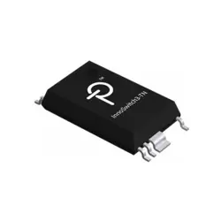
画像は参照用のみです。
LNK606DG
IC OFFLINE SWITCH FLYBACK 8SO
- メーカー
- Mfr。パート #LNK606DG
- パッケージ
- データシート LNK606DG DataSheet
- 在庫中6875
100% オリジナル &新しい
出荷の準備ができている24時間
365日の保証
RFQおよびもっと割引を得る
仕様
| Series | LinkSwitch®-II |
| Part Status | Discontinued at DigiKey |
| Base Product Number | LNK606 |
| Output Isolation | Isolated |
| Internal Switch(s) | Yes |
| Voltage - Breakdown | 700V |
| Topology | Flyback |
| Duty Cycle | 55% |
| Frequency - Switching | Up to 85kHz |
| Fault Protection | Current Limiting, Open Loop, Over Temperature, Short Circuit |
| Operating Temperature | -40°C ~ 150°C (TJ) |
| Package | 8-SOIC (0.154", 3.90mm Width), 7 Leads |
| Supplier Device Package | SO-8C |
| Mounting Type | Surface Mount |
| Packaging | Tube |
| Power (Watts) | 6.1 W |
概要
Description
The LNK606DG is a member of the LinkSwitch-II family, which are highly integrated monolithic switching ICs designed by Power Integrations for energy-efficient AC-DC power conversion. This specific model is often used in low-power applications such as chargers, adapters, and consumer electronics. Key features of the LNK606DG include its ability to deliver accurate constant voltage (CV) and constant current (CC) regulation, along with excellent efficiency. It incorporates a 700V power MOSFET, oscillator, on/off control, a high-voltage switched current source, frequency jittering, cycle-by-cycle current limit, and thermal shutdown circuitry, all within a single chip.
The LNK606DG simplifies design by reducing component count and enhancing reliability through its integrated approach. It operates over a wide input voltage range and supports both flyback and buck converter topologies. The IC also supports silent operation with its low EMI design, which avoids audible noise. Furthermore, it helps in meeting global energy efficiency standards due to its low standby power consumption. This makes the LNK606DG suitable for modern electronic devices requiring both compact size and high efficiency.
The LNK606DG simplifies design by reducing component count and enhancing reliability through its integrated approach. It operates over a wide input voltage range and supports both flyback and buck converter topologies. The IC also supports silent operation with its low EMI design, which avoids audible noise. Furthermore, it helps in meeting global energy efficiency standards due to its low standby power consumption. This makes the LNK606DG suitable for modern electronic devices requiring both compact size and high efficiency.
Features
The LNK606DG is an integrated circuit designed for energy-efficient power supply applications. It is part of the LinkSwitch-II family from Power Integrations, known for simplifying the design of flyback, buck, and boost converters. Key features of the LNK606DG include:
1. Energy Efficiency: It offers high efficiency across the load range, minimizing energy consumption in both active and standby modes.
2. Integrated Controller: The IC combines a controller with a high-voltage power MOSFET, reducing the need for external components and simplifying circuit design.
3. Accurate Regulation: It provides excellent voltage regulation, often without the need for a secondary feedback circuit, thanks to its primary-side control.
4. Protection Features: Includes comprehensive safety features such as over-temperature, over-current, and over-voltage protection to enhance reliability.
5. Design Flexibility: Suitable for various power supply configurations, including isolated and non-isolated topologies.
6. Compact Package: Available in a compact SMD package, which is ideal for space-constrained applications.
7. Wide Input Voltage Range: Supports a broad input voltage range, making it versatile for global applications.
These features make the LNK606DG suitable for a wide range of applications, including chargers, adapters, appliances, and industrial products.
1. Energy Efficiency: It offers high efficiency across the load range, minimizing energy consumption in both active and standby modes.
2. Integrated Controller: The IC combines a controller with a high-voltage power MOSFET, reducing the need for external components and simplifying circuit design.
3. Accurate Regulation: It provides excellent voltage regulation, often without the need for a secondary feedback circuit, thanks to its primary-side control.
4. Protection Features: Includes comprehensive safety features such as over-temperature, over-current, and over-voltage protection to enhance reliability.
5. Design Flexibility: Suitable for various power supply configurations, including isolated and non-isolated topologies.
6. Compact Package: Available in a compact SMD package, which is ideal for space-constrained applications.
7. Wide Input Voltage Range: Supports a broad input voltage range, making it versatile for global applications.
These features make the LNK606DG suitable for a wide range of applications, including chargers, adapters, appliances, and industrial products.
Package
The LNK606DG is housed in an SMD-8 package, which is a surface-mount package with 8 pins. This type of package is commonly used for efficient assembly on printed circuit boards (PCBs) in power supply applications.
Pinout
The LNK606DG is part of the LinkSwitch-II series by Power Integrations, designed for low-power, high-efficiency off-line switcher applications such as chargers and adapters. It comes in an 8-pin SO-8 (Surface-Mount) package.
The pin functions are as follows:
1. BP (Bypass Pin): Connects to an external capacitor for internal supply voltage stabilization.
2. S (Source): The circuit common or ground reference pin.
3. D (Drain): High-voltage power MOSFET drain connection. It connects to the primary winding of the transformer.
4. FB (Feedback): Used for output voltage regulation by connecting to the output feedback network.
5. S (Source): Another source pin, as the device typically has multiple source connections for better current carrying capability.
6. S (Source): Same as above.
7. S (Source): Same as above.
8. S (Source): Same as above.
The LNK606DG integrates a high-voltage power MOSFET, oscillator, high-voltage switched current source, current limit, and thermal shutdown circuitry onto a single IC. This integration helps in reducing component count and improving design efficiency.
The pin functions are as follows:
1. BP (Bypass Pin): Connects to an external capacitor for internal supply voltage stabilization.
2. S (Source): The circuit common or ground reference pin.
3. D (Drain): High-voltage power MOSFET drain connection. It connects to the primary winding of the transformer.
4. FB (Feedback): Used for output voltage regulation by connecting to the output feedback network.
5. S (Source): Another source pin, as the device typically has multiple source connections for better current carrying capability.
6. S (Source): Same as above.
7. S (Source): Same as above.
8. S (Source): Same as above.
The LNK606DG integrates a high-voltage power MOSFET, oscillator, high-voltage switched current source, current limit, and thermal shutdown circuitry onto a single IC. This integration helps in reducing component count and improving design efficiency.
Manufacturer
The LNK606DG is manufactured by Power Integrations, Inc. This company specializes in developing high-performance electronic components used in high voltage power conversion. Power Integrations focuses on energy-efficient solutions and produces integrated circuits that are widely used in power supplies and chargers for a variety of electronic devices. Their products emphasize reducing energy consumption and simplifying power supply designs.
Application
The LNK606DG is typically used in power supply design, specifically for off-line switch-mode power supplies. Its application areas include compact chargers, adapters for consumer electronics, LED drivers, and home appliances. It is valued for its high efficiency, low standby power consumption, and ability to reduce the overall component count and cost in power supply designs.
Equivalent
Equivalent products to the LNK606DG chip, used for AC-DC power conversion, include the NCP1014 from ON Semiconductor, VIPer12A from STMicroelectronics, and TNY280PG from Power Integrations. These chips serve similar functions in power supply applications, but always check specifications and datasheets for compatibility with your specific requirements.
出荷
出荷方法私たち
DHL、FedEx、TNT、UPS、またはあなたの選択の他の運送業者を通じてグローバルな出荷サービスを提供します。
出荷料参照(DHL/FedEx):
DHL の: 配送費は25ドル〜45ドル(0.5kg)の範囲で、推定配送時間は2〜5営業日です。
フェデックス: 配送費は25ドル〜40ドル(0.5kg)の範囲で、推定配送時間は3〜7営業日。
UPS の: 配送費は25ドル〜45ドル(0.5kg)の範囲で、推定配送時間は3〜7営業日。
TNT社: 配送費は25ドル〜65ドル(0.5kg)の範囲で、推定配送時間は3〜7営業日。
EMS: 配送料金は30〜50ドル(0.5kg)の範囲で、推定配送時間は7〜15営業日です。
登録航空郵便: 配送費は2〜4ドル(0.1kg)で、推定配送時間は5〜20営業日です。
支払い
Payment Methods
支払い期間は100%前払いです。
現在、下記の支払い方法のみを受け入れています。:
1. ペイパル
2. クレジット・デビットカード
3. ワイヤー 転送
類似
-
![MX25L3233FZBI-08Q]() MX25L3233FZBI-08Q
Macronix
-
![MX25V1635FZNQ03]() MX25V1635FZNQ03
Macronix
-
![MX25V2033FM1I]() MX25V2033FM1I
Macronix
-
![MX30LF2G28AD-TI]() MX30LF2G28AD-TI
Macronix
-
![MX25R6435FBDIL0]() MX25R6435FBDIL0
Macronix
-
![MX25U3232FZBI02]() MX25U3232FZBI02
Macronix
-
![MX25L6433FM2I-08G]() MX25L6433FM2I-08G
Macronix
-
![MX25L12833FZ2I-10G]() MX25L12833FZ2I-10..
Macronix
-
![MX25L12833FZNI-10G]() MX25L12833FZNI-10..
Macronix
-
![MX25L12835FZ2I-10G]() MX25L12835FZ2I-10..
Macronix
-
![MX29LV640ETTI-70G]() MX29LV640ETTI-70G
Macronix
-
![MX66U1G45GMI00]() MX66U1G45GMI00
Macronix