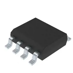
画像は参照用のみです。
L2N7002LT1G
MOSFETs
- メーカー
- Mfr。パート #L2N7002LT1G
- パッケージ
- データシート
- 在庫中20908
100% オリジナル &新しい
出荷の準備ができている24時間
365日の保証
RFQおよびもっと割引を得る
仕様
概要
Description
The L2N7002LT1G is an N-channel MOSFET (Metal-Oxide-Semiconductor Field-Effect Transistor) designed for low-voltage applications. It features a low on-resistance (R_DS(on)) of approximately 0.5 ohms, making it efficient for switching and amplification tasks. The device can handle a maximum drain current of 2A and has a drain-source voltage rating of 60V, which allows it to be used in various power management applications.
This MOSFET is particularly valued for its fast switching speeds and low gate threshold voltage, enabling it to operate effectively with low drive voltages. With its small (SOT-23) package, it’s suitable for space-constrained designs, including portable devices, power supplies, and motor control circuits. It also offers thermal stability and robustness, making it a reliable choice for engineers in circuit design. Overall, the L2N7002LT1G is a versatile component widely used in consumer electronics and industrial applications.
This MOSFET is particularly valued for its fast switching speeds and low gate threshold voltage, enabling it to operate effectively with low drive voltages. With its small (SOT-23) package, it’s suitable for space-constrained designs, including portable devices, power supplies, and motor control circuits. It also offers thermal stability and robustness, making it a reliable choice for engineers in circuit design. Overall, the L2N7002LT1G is a versatile component widely used in consumer electronics and industrial applications.
Features
The L2N7002LT1G is an N-channel MOSFET designed for low-voltage applications. Key features include:
1. Voltage Rating: It supports a maximum drain-source voltage (V_DS) of 60V.
2. Current Handling: It can handle a continuous drain current (I_D) up to 0.5A.
3. R_DS(on): Offers low on-resistance of approximately 0.5 ohms at V_GS = 10V, enhancing efficiency.
4. Gate Threshold Voltage: The gate-source threshold voltage (V_GS(th)) ranges from 1V to 3V, making it suitable for low-voltage drive applications.
5. Package: Available in a compact SOT-23 package, suitable for space-constrained designs.
6. Fast Switching: Ideal for switching applications due to its fast switching speeds.
7. Applications: Commonly used in low-side switches, load switching, and other general-purpose applications.
These features make the L2N7002LT1G a versatile choice for various electronic applications requiring efficient switching.
Package
The L2N7002LT1G is packaged in a small SOT-23 surface mount package. This compact design is ideal for space-constrained applications in electronic circuits.
Pinout
The L2N7002LT1G is a small signal N-channel MOSFET with a pin count of 3. The pin functions are as follows:
1. Gate (G): This pin is used to control the MOSFET. A voltage applied to the gate turns the device on, allowing current to flow from the drain to the source.
2. Drain (D): This is the output pin where the load is connected. Current flows from the drain to the source when the MOSFET is in the "on" state.
3. Source (S): This pin is typically connected to ground (or the negative side of the power supply) in common-source configurations. It serves as the reference point for current flow through the device.
The L2N7002LT1G is commonly used in low-power switching applications, where its compact size and efficiency make it suitable for various electronic circuits.
Manufacturer
The L2N7002LT1G is manufactured by ON Semiconductor, a global semiconductor company. ON Semiconductor specializes in providing a wide range of semiconductor solutions, including analog, digital, and mixed-signal devices. They focus on enabling energy-efficient electronics and serving various markets, including automotive, industrial, consumer, and telecommunications. The company is known for its commitment to innovation and sustainability in the semiconductor industry, offering products that enhance performance while reducing power consumption.
Application
The L2N7002LT1G is an N-channel MOSFET commonly used in low-power switching applications. Its application areas include power management circuits, load switching, signal switching, and general-purpose amplification. It is suitable for driving low-current loads in battery-powered devices, consumer electronics, and automotive applications due to its low on-resistance and high switching speeds.
Equivalent
Equivalent products to the L2N7002LT1G include the 2N7000, 2N7002, BS170, and MMBT3904 MOSFETs. These alternatives share similar characteristics such as voltage, current ratings, and package types, though specific parameters may vary. Always consult datasheets to ensure compatibility for your application.
出荷
出荷方法私たち
DHL、FedEx、TNT、UPS、またはあなたの選択の他の運送業者を通じてグローバルな出荷サービスを提供します。
出荷料参照(DHL/FedEx):
DHL の: 配送費は25ドル〜45ドル(0.5kg)の範囲で、推定配送時間は2〜5営業日です。
フェデックス: 配送費は25ドル〜40ドル(0.5kg)の範囲で、推定配送時間は3〜7営業日。
UPS の: 配送費は25ドル〜45ドル(0.5kg)の範囲で、推定配送時間は3〜7営業日。
TNT社: 配送費は25ドル〜65ドル(0.5kg)の範囲で、推定配送時間は3〜7営業日。
EMS: 配送料金は30〜50ドル(0.5kg)の範囲で、推定配送時間は7〜15営業日です。
登録航空郵便: 配送費は2〜4ドル(0.1kg)で、推定配送時間は5〜20営業日です。
支払い
Payment Methods
支払い期間は100%前払いです。
現在、下記の支払い方法のみを受け入れています。:
1. ペイパル
2. クレジット・デビットカード
3. ワイヤー 転送
類似
-
![MX25V1635FZNI]() MX25V1635FZNI
Macronix
-
![MX29F400CBTI-70G]() MX29F400CBTI-70G
Macronix
-
![MX25V2033FM1I]() MX25V2033FM1I
Macronix
-
![MX25V16066M1I02]() MX25V16066M1I02
Macronix
-
![MX25R3235FZNIL0]() MX25R3235FZNIL0
Macronix
-
![MX25V16066M2I02]() MX25V16066M2I02
Macronix
-
![MX25L25673GMI-08G]() MX25L25673GMI-08G
Macronix
-
![MX25L25673GMI-10G]() MX25L25673GMI-10G
Macronix
-
![MX29GL512FHXFI-11G]() MX29GL512FHXFI-11..
Macronix
-
![MX25U51279GXDR00]() MX25U51279GXDR00
Macronix
-
![MX25V1635FM2I]() MX25V1635FM2I
Macronix
-
![MX25L12833FM2I-10G]() MX25L12833FM2I-10..
Macronix