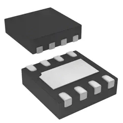
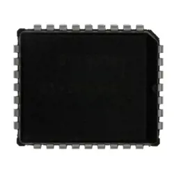
画像は参照用のみです。
JS28F256P33TFE
NOR Flash PARALLEL NOR MLC 16MX16 TSOP
- メーカー
- Mfr。パート #JS28F256P33TFE
- パッケージ
- データシート
- 在庫中10104
100% オリジナル &新しい
出荷の準備ができている24時間
365日の保証
RFQおよびもっと割引を得る
仕様
| Packaging | Tray |
| Standard Pack Qty | 576 |
概要
Description
The JS28F256P33TFE is a 256Mb (32MB) NOR Flash memory device manufactured by Macronix, designed for embedded applications. It features a parallel interface, allowing for high-speed data access and easy integration into various electronic systems. The device operates at a supply voltage of 2.7V to 3.6V, making it suitable for low-power applications.
Key specifications include fast read speeds, with access times typically around 70 ns, and support for multiple programming and erase modes. The Flash memory is organized in a way that enables efficient data storage and retrieval, with block erase and byte write capabilities.
The JS28F256P33TFE is commonly used in automotive, industrial, and consumer electronics for firmware storage, providing reliable performance and endurance suitable for critical applications. Its robustness and longevity make it a preferred choice for applications that require non-volatile memory solutions.
Package
The JS28F256P33TFE is packaged in a TSOP (Thin Small Outline Package) type. It features a 48-pin configuration, suitable for surface mount applications, providing a compact design for efficient space utilization on PCBs.
Pinout
The JS28F256P33TFE is a 256Mb (32MB) NAND Flash memory device, typically in a TSOP (Thin Small Outline Package) form factor. It has a pin count of 48 pins.
The primary functions of these pins include:
1. Data Bus (DQ0-DQ7): 8-bit data input/output for read/write operations.
2. Address Bus (A0-A21): Used to select specific memory locations.
3. Control Signals:
- CE# (Chip Enable): Activates the device.
- WE# (Write Enable): Initiates write operations.
- OE# (Output Enable): Controls data output during read operations.
- RE# (Read Enable): Triggers read operations.
4. Status and Control:
- R/B# (Ready/Busy): Indicates the status of the device.
- WP# (Write Protect): Protects against accidental writing.
5. Power Supply and Ground: Pins for Vcc and GND connections.
This device is commonly used in consumer electronics, embedded systems, and applications requiring non-volatile storage.
Manufacturer
The JS28F256P33TFE is manufactured by Micron Technology, Inc. Micron is a leading American semiconductor company that specializes in memory and storage solutions, including DRAM and NAND flash memory. Founded in 1978, Micron designs and produces a wide range of products used in various applications, such as computing, mobile devices, and automotive electronics. The company is known for its innovation in memory technology and plays a significant role in the global semiconductor industry.
Application
The JS28F256P33TFE is a NAND flash memory device commonly used in applications such as mobile devices, consumer electronics, automotive systems, and industrial equipment. It is suitable for data storage, firmware updates, multimedia applications, and embedded systems requiring high-density, non-volatile memory solutions. Its features include fast read/write speeds and reliable performance in various temperature ranges.
Equivalent
The JS28F256P33TFE chip is a 256Mb NOR Flash memory. Equivalent products include the Micron MT28EW256ABA, Winbond W25Q256, and Spansion S25FL256S. Always verify compatibility regarding pin configuration, voltage levels, and performance specifications before substitution.
出荷
出荷方法私たち
DHL、FedEx、TNT、UPS、またはあなたの選択の他の運送業者を通じてグローバルな出荷サービスを提供します。
出荷料参照(DHL/FedEx):
DHL の: 配送費は25ドル〜45ドル(0.5kg)の範囲で、推定配送時間は2〜5営業日です。
フェデックス: 配送費は25ドル〜40ドル(0.5kg)の範囲で、推定配送時間は3〜7営業日。
UPS の: 配送費は25ドル〜45ドル(0.5kg)の範囲で、推定配送時間は3〜7営業日。
TNT社: 配送費は25ドル〜65ドル(0.5kg)の範囲で、推定配送時間は3〜7営業日。
EMS: 配送料金は30〜50ドル(0.5kg)の範囲で、推定配送時間は7〜15営業日です。
登録航空郵便: 配送費は2〜4ドル(0.1kg)で、推定配送時間は5〜20営業日です。
支払い
Payment Methods
支払い期間は100%前払いです。
現在、下記の支払い方法のみを受け入れています。:
1. ペイパル
2. クレジット・デビットカード
3. ワイヤー 転送
類似
-
![MX25L3233FM1I-08Q]() MX25L3233FM1I-08Q
Macronix
-
![MX29F400CBTI-70G]() MX29F400CBTI-70G
Macronix
-
![MX25V16066M1I02]() MX25V16066M1I02
Macronix
-
![MX25R3235FZNIL0]() MX25R3235FZNIL0
Macronix
-
![MX29GL512FHXFI-11G]() MX29GL512FHXFI-11..
Macronix
-
![MX25U25643GZNI00]() MX25U25643GZNI00
Macronix
-
![MX25L2006EM1I-12G]() MX25L2006EM1I-12G
Macronix
-
![MX25R1635FZUIH0]() MX25R1635FZUIH0
Macronix
-
![MX25L12833FZ2I-10G]() MX25L12833FZ2I-10..
Macronix
-
![MX25L12833FZNI-10G]() MX25L12833FZNI-10..
Macronix
-
![MX29F040CQI-70G]() MX29F040CQI-70G
Macronix
-
![MX25L25645GXDI-08G]() MX25L25645GXDI-08..
Macronix