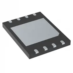
画像は参照用のみです。
IS42S16160J-7BLI
IC DRAM 256MBIT PARALLEL 54TFBGA
- メーカー
- Mfr。パート #IS42S16160J-7BLI
- パッケージ BGA-54
- データシート IS42S16160J-7BLI DataSheet
- 在庫中5481
100% オリジナル &新しい
出荷の準備ができている24時間
365日の保証
RFQおよびもっと割引を得る
仕様
| Package | Tray |
| ProductStatus | Active |
| MemoryType | Volatile |
| MemoryFormat | DRAM |
| Technology | SDRAM |
| MemorySize | 256Mb (16M x 16) |
| MemoryInterface | Parallel |
| ClockFrequency | 143 MHz |
| AccessTime | 5.4 ns |
| Voltage-Supply | 3V ~ 3.6V |
| OperatingTemperature | -40°C ~ 85°C (TA) |
| MountingType | Surface Mount |
| Package/Case | 54-TFBGA |
概要
Description
The IS42S16160J-7BLI is a 16M x 16-bit synchronous dynamic random-access memory (SDRAM) chip manufactured by ISSI (Integrated Silicon Solution, Inc.). It operates at a voltage of 3.3V and features a data rate of up to 133 MHz, making it suitable for various applications requiring fast data processing, such as networking and telecommunications equipment, consumer electronics, and embedded systems.
This SDRAM is designed to support burst mode operations, which enhances data transfer rates, and it includes features like programmable burst lengths and an advanced power-saving mode to improve efficiency. The "7BLI" suffix indicates specific features related to the package type and operating temperature range, making it suitable for industrial applications.
Overall, the IS42S16160J-7BLI is known for its reliability and performance in high-speed memory applications.
This SDRAM is designed to support burst mode operations, which enhances data transfer rates, and it includes features like programmable burst lengths and an advanced power-saving mode to improve efficiency. The "7BLI" suffix indicates specific features related to the package type and operating temperature range, making it suitable for industrial applications.
Overall, the IS42S16160J-7BLI is known for its reliability and performance in high-speed memory applications.
Features
The IS42S16160J-7BLI is a 16Mb (2M x 8) asynchronous SRAM memory chip. Key features include:
1. Access Time: 70 ns typical access time, allowing for fast data retrieval.
2. Voltage Supply: Operates at a supply voltage of 2.7V to 3.6V.
3. Low Power Consumption: Designed for low power usage, making it suitable for battery-operated devices.
4. Asynchronous Operation: Supports asynchronous read and write operations, simplifying interfacing in various applications.
5. Wide Operating Temperature Range: Typically from -40°C to +85°C, suitable for industrial applications.
6. Compatibility: Pin-compatible with other similar SRAMs, allowing for easy integration.
7. Packaging: Available in a 48-pin TSOP package, convenient for PCB design.
This chip is ideal for applications requiring fast memory access, such as networking, telecommunications, and consumer electronics.
1. Access Time: 70 ns typical access time, allowing for fast data retrieval.
2. Voltage Supply: Operates at a supply voltage of 2.7V to 3.6V.
3. Low Power Consumption: Designed for low power usage, making it suitable for battery-operated devices.
4. Asynchronous Operation: Supports asynchronous read and write operations, simplifying interfacing in various applications.
5. Wide Operating Temperature Range: Typically from -40°C to +85°C, suitable for industrial applications.
6. Compatibility: Pin-compatible with other similar SRAMs, allowing for easy integration.
7. Packaging: Available in a 48-pin TSOP package, convenient for PCB design.
This chip is ideal for applications requiring fast memory access, such as networking, telecommunications, and consumer electronics.
Package
The IS42S16160J-7BLI is a DRAM memory chip packaged in a 54-pin TSOP II (Thin Small Outline Package) configuration. This package type is commonly used for memory devices, providing a compact design suitable for various electronic applications.
Pinout
The IS42S16160J-7BLI is a 16 Meg x 16 bit (256 Megabit) synchronous dynamic random-access memory (SDRAM) chip. It has a total pin count of 54 pins.
The primary functions of these pins include:
- Data Pins (DQ0-DQ15): 16 data lines for input/output.
- Address Pins (A0-A11): Used for addressing the memory locations.
- Control Pins:
- Chip Select (CS): Activates the chip.
- Write Enable (WE): Enables write operations.
- Read Enable (OE): Enables read operations.
- Clock (CLK): Synchronizes data transfer.
- Clock Enable (CEN): Enables/disables the clock.
- Baud Pins (BA0, BA1): Select between different memory banks.
- Refresh Pins (REF): Used for refreshing the memory.
- Power and Ground Pins (VDD, VSS): Power supply and ground connections.
This chip is typically used in applications requiring high-speed memory access.
The primary functions of these pins include:
- Data Pins (DQ0-DQ15): 16 data lines for input/output.
- Address Pins (A0-A11): Used for addressing the memory locations.
- Control Pins:
- Chip Select (CS): Activates the chip.
- Write Enable (WE): Enables write operations.
- Read Enable (OE): Enables read operations.
- Clock (CLK): Synchronizes data transfer.
- Clock Enable (CEN): Enables/disables the clock.
- Baud Pins (BA0, BA1): Select between different memory banks.
- Refresh Pins (REF): Used for refreshing the memory.
- Power and Ground Pins (VDD, VSS): Power supply and ground connections.
This chip is typically used in applications requiring high-speed memory access.
Manufacturer
The IS42S16160J-7BLI is manufactured by ISSI (Integrated Silicon Solution, Inc.), which is a semiconductor company specializing in high-performance memory products. Founded in 1988, ISSI designs and manufactures a variety of memory solutions, including SRAM, DRAM, and Flash memory. The company focuses on serving markets such as telecommunications, automotive, consumer electronics, and industrial applications. ISSI is known for its commitment to quality and innovation in the memory industry, providing reliable and cost-effective solutions for its customers.
Application
The IS42S16160J-7BLI is a 16Mb (2M x 8) SDRAM memory chip used in various applications, including consumer electronics, mobile devices, networking equipment, and embedded systems. Its features support high-speed data processing, making it suitable for applications like graphics processing, gaming consoles, and industrial automation where efficient memory access is crucial.
Equivalent
The IS42S16160J-7BLI chip is a 1Gb DDR SDRAM (Double Data Rate Synchronous Dynamic Random Access Memory) component. Equivalent products include:
1. MT46V16M16TG-7 (Micron)
2. Hynix H5TQ1G63AFR (SK Hynix)
3. K4T1G164EB-HCE7 (Samsung)
Always verify compatibility with your specific application requirements.
1. MT46V16M16TG-7 (Micron)
2. Hynix H5TQ1G63AFR (SK Hynix)
3. K4T1G164EB-HCE7 (Samsung)
Always verify compatibility with your specific application requirements.
出荷
出荷方法私たち
DHL、FedEx、TNT、UPS、またはあなたの選択の他の運送業者を通じてグローバルな出荷サービスを提供します。
出荷料参照(DHL/FedEx):
DHL の: 配送費は25ドル〜45ドル(0.5kg)の範囲で、推定配送時間は2〜5営業日です。
フェデックス: 配送費は25ドル〜40ドル(0.5kg)の範囲で、推定配送時間は3〜7営業日。
UPS の: 配送費は25ドル〜45ドル(0.5kg)の範囲で、推定配送時間は3〜7営業日。
TNT社: 配送費は25ドル〜65ドル(0.5kg)の範囲で、推定配送時間は3〜7営業日。
EMS: 配送料金は30〜50ドル(0.5kg)の範囲で、推定配送時間は7〜15営業日です。
登録航空郵便: 配送費は2〜4ドル(0.1kg)で、推定配送時間は5〜20営業日です。
支払い
Payment Methods
支払い期間は100%前払いです。
現在、下記の支払い方法のみを受け入れています。:
1. ペイパル
2. クレジット・デビットカード
3. ワイヤー 転送
類似
-
![MX25R8035FM1IL0]() MX25R8035FM1IL0
Macronix
-
![MX25L3233FZBI-08Q]() MX25L3233FZBI-08Q
Macronix
-
![MX25V1635FZNI]() MX25V1635FZNI
Macronix
-
![MX66U1G45GXDI00]() MX66U1G45GXDI00
Macronix
-
![MX25V5126FM1I]() MX25V5126FM1I
Macronix
-
![MX25V4035FZUI]() MX25V4035FZUI
Macronix
-
![MX25L25673GMI-10G]() MX25L25673GMI-10G
Macronix
-
![MX25L2006EM1I-12G]() MX25L2006EM1I-12G
Macronix
-
![MX25V1635FM2I]() MX25V1635FM2I
Macronix
-
![MX25U3232FZBI02]() MX25U3232FZBI02
Macronix
-
![MX25L12833FZNI-10G]() MX25L12833FZNI-10..
Macronix
-
![MX25L12835FZ2I-10G]() MX25L12835FZ2I-10..
Macronix