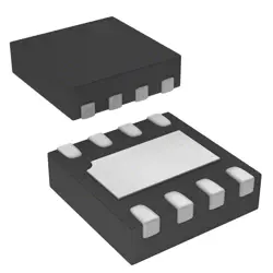
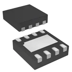
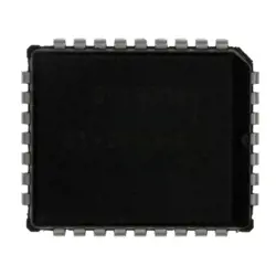
画像は参照用のみです。
IS21ES32G-JCLI
IC FLASH 256GBIT EMMC 153VFBGA
- メーカー
- Mfr。パート #IS21ES32G-JCLI
- パッケージ
- データシート
- 在庫中7889
100% オリジナル &新しい
出荷の準備ができている24時間
365日の保証
RFQおよびもっと割引を得る
仕様
| Part Status | Discontinued at DigiKey |
| Base Product Number | IS21ES32 |
| DigiKey Programmable | Not Verified |
| Memory Type | Non-Volatile |
| Memory Format | FLASH |
| Technology | FLASH - NAND (MLC) |
| Memory Size | 256Gbit |
| Memory Organization | 32G x 8 |
| Memory Interface | eMMC |
| Clock Frequency | 200 MHz |
| Voltage - Supply | 2.7V ~ 3.6V |
| Operating Temperature | -40°C ~ 85°C (TA) |
| Mounting Type | Surface Mount |
| Package | 153-VFBGA |
| Supplier Device Package | 153-VFBGA (11.5x13) |
| Packaging | Tray |
概要
Description
The IS21ES32G-JCLI is a high-performance, low-power CMOS static random-access memory (SRAM) chip designed for various applications in consumer electronics, automotive systems, and industrial devices. It features a 32 megabit capacity, organized as 4M x 8 bits, enabling efficient data storage and retrieval. The chip operates at a wide voltage range, typically around 1.8V to 3.6V, making it suitable for battery-powered devices where energy efficiency is critical.
Key features include fast access times, typically around 70 ns, and a simple interface for easy integration into existing systems. The IS21ES32G also supports various modes, such as standby and active read/write modes, to optimize power consumption. Additionally, it is designed with robust reliability features, including error correction codes (ECC) to ensure data integrity over time.
The device is packaged in a compact 48-ball FBGA, facilitating space-saving designs in modern electronics. Overall, the IS21ES32G-JCLI is ideal for applications requiring quick data access and low power consumption, making it a popular choice in the SRAM market.
Features
The IS21ES32G-JCLI is a 32Mb (4MB) CMOS SRAM (Static Random Access Memory) chip designed for high-speed data storage. Key features include:
1. Memory Density: 32Mb capacity, suitable for various applications.
2. Access Time: Fast access times, typically around 55ns, allowing quick data retrieval.
3. Low Power Consumption: Operates at low voltage, enhancing energy efficiency.
4. Asynchronous Operation: Supports asynchronous read and write cycles, simplifying integration into systems.
5. Wide Operating Voltage: Compatible with a range of supply voltages, often between 2.7V to 3.6V.
6. Integrated Control Functions: Built-in control signals for easy interfacing with microcontrollers and processors.
7. Temperature Range: Designed to operate over a broad temperature range, making it suitable for various environments.
These features make the IS21ES32G-JCLI ideal for applications in telecommunications, automotive, and industrial control systems where reliable, high-speed memory is crucial.
Package
The IS21ES32G-JCLI is packaged in a 48-ball FBGA (Fine Ball Grid Array) format. This type of packaging is designed for efficient space utilization and improved thermal performance, making it suitable for various applications in electronic devices.
Pinout
The IS21ES32G-JCLI is a 32M-bit (4M x 8-bit) NAND Flash memory device. It typically has a 48-pin configuration. The main functions of these pins include:
1. Data Pins (DQ0-DQ7): These are the 8 data input/output pins used for reading and writing data.
2. Address Pins (A0-A19): These pins are used to address memory locations within the chip.
3. Control Pins:
- CE (Chip Enable): Activates the chip for read/write operations.
- WE (Write Enable): Initiates write operations.
- RE (Read Enable): Initiates read operations.
- WP (Write Protect): Protects the memory from accidental writes.
4. Status Pins: These may include RQST (Request) or other status indicators depending on the specific configuration.
The device supports various operations such as random access, read, and write commands, making it suitable for various applications in embedded systems.
Manufacturer
The IS21ES32G-JCLI is manufactured by Integrated Silicon Solution, Inc. (ISSI), which is a company specializing in semiconductor products. Founded in 1988 and headquartered in San Jose, California, ISSI focuses on designing and manufacturing high-performance memory and analog integrated circuits. Their product lines include SRAM, DRAM, and Flash memory, catering to various applications in automotive, consumer electronics, telecommunications, and industrial markets. ISSI is recognized for its commitment to innovation and quality in the semiconductor industry.
Application
The IS21ES32G-JCLI is a high-performance, low-power DDR3 SDRAM memory chip commonly used in various application areas, including consumer electronics, automotive systems, industrial equipment, and networking devices. It supports high-speed data processing and is ideal for applications requiring efficient memory usage, such as smartphones, tablets, embedded systems, and IoT devices. Its robust performance and reliability make it suitable for both commercial and industrial environments.
Equivalent
The IS21ES32G-JCLI chip is a 32Mb (4MB) CMOS SRAM. Equivalent products include the Micron MT41J128M16HA-125, Cypress CY7C1361G, and ISSI IS61WV25616BLL-10T. These alternatives may vary in specifications such as speed, voltage, and packaging, so it’s important to check compatibility for specific applications.
出荷
出荷方法私たち
DHL、FedEx、TNT、UPS、またはあなたの選択の他の運送業者を通じてグローバルな出荷サービスを提供します。
出荷料参照(DHL/FedEx):
DHL の: 配送費は25ドル〜45ドル(0.5kg)の範囲で、推定配送時間は2〜5営業日です。
フェデックス: 配送費は25ドル〜40ドル(0.5kg)の範囲で、推定配送時間は3〜7営業日。
UPS の: 配送費は25ドル〜45ドル(0.5kg)の範囲で、推定配送時間は3〜7営業日。
TNT社: 配送費は25ドル〜65ドル(0.5kg)の範囲で、推定配送時間は3〜7営業日。
EMS: 配送料金は30〜50ドル(0.5kg)の範囲で、推定配送時間は7〜15営業日です。
登録航空郵便: 配送費は2〜4ドル(0.1kg)で、推定配送時間は5〜20営業日です。
支払い
Payment Methods
支払い期間は100%前払いです。
現在、下記の支払い方法のみを受け入れています。:
1. ペイパル
2. クレジット・デビットカード
3. ワイヤー 転送
類似
-
![MX25R8035FM1IL0]() MX25R8035FM1IL0
Macronix
-
![MX25L3233FM1I-08Q]() MX25L3233FM1I-08Q
Macronix
-
![MX25V2033FM1I]() MX25V2033FM1I
Macronix
-
![MX25R3235FZNIL0]() MX25R3235FZNIL0
Macronix
-
![MX25L8035EM2I-10G]() MX25L8035EM2I-10G
Macronix
-
![MX25L25673GMI-10G]() MX25L25673GMI-10G
Macronix
-
![MX25R1635FZUIH0]() MX25R1635FZUIH0
Macronix
-
![MX25U3232FZBI02]() MX25U3232FZBI02
Macronix
-
![MX25L12833FZ2I-10G]() MX25L12833FZ2I-10..
Macronix
-
![MX25L12833FZNI-10G]() MX25L12833FZNI-10..
Macronix
-
![MX25U25645GXDI00]() MX25U25645GXDI00
Macronix
-
![MX29F040CQI-70G]() MX29F040CQI-70G
Macronix