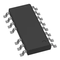
画像は参照用のみです。
HCF4094BE
- メーカー
- Mfr。パート #HCF4094BE
- パッケージ
- データシート
- 在庫中6926
100% オリジナル &新しい
出荷の準備ができている24時間
365日の保証
RFQおよびもっと割引を得る
仕様
| Manufacturer | STMicroelectronics |
| Package | DIP-16 |
概要
Description
The HCF4094BE is an integrated circuit from the CMOS logic family, specifically designed for digital applications. It is a shift register with a 3-state serial output. The component consists of an 8-stage shift-and-store register, with a storage latch associated with each stage for strobing data from the serial input to parallel output. This dual-purpose register enables both serial data input and parallel data output, making it useful in applications requiring a compact serial-to-parallel data conversion.
Key features include a serial data input, a clock input for data shifting, and a strobe input for latching the data. The device outputs include 8 parallel data outputs and a serial output for cascading additional registers. It operates with a wide supply voltage range from 3V to 15V, making it versatile for various electronic projects. The HCF4094BE is typically used in LED display drivers, digital data storage, and control systems where efficient data manipulation is required. The device is lauded for its low power consumption and high noise immunity, traits typical of CMOS technology.
Key features include a serial data input, a clock input for data shifting, and a strobe input for latching the data. The device outputs include 8 parallel data outputs and a serial output for cascading additional registers. It operates with a wide supply voltage range from 3V to 15V, making it versatile for various electronic projects. The HCF4094BE is typically used in LED display drivers, digital data storage, and control systems where efficient data manipulation is required. The device is lauded for its low power consumption and high noise immunity, traits typical of CMOS technology.
Features
The HCF4094BE is a silicon gate CMOS device commonly used as an 8-stage shift-and-store register. Key features include:
1. 8-Bit Shift Register and Latch: It combines an 8-bit shift register with a data latch and a 3-state output.
2. High-Speed Operation: The device can handle high-speed operations due to its fast switching characteristics.
3. Low Power Consumption: Being a CMOS device, it has low power consumption, making it suitable for battery-powered applications.
4. Wide Supply Voltage Range: It operates over a wide voltage range, typically from 3V to 15V, enhancing its versatility.
5. 3-State Outputs: The outputs can be set to high, low, or high-impedance states, allowing for bus interfacing.
6. Serial Input and Output: It supports serial data input and output, enabling easy cascading of multiple devices for extended data storage.
7. Latch Enable Input: It allows data to be latched, holding it for further processing or output.
These features make the HCF4094BE suitable for applications requiring serial-to-parallel conversion, data storage, and light control in low-power environments.
Package
The HCF4094BE is a shift register IC and is typically available in a Dual In-line Package (DIP) with 16 pins. This package type is widely used for through-hole mounting on printed circuit boards (PCBs).
Pinout
The HCF4094BE is a CMOS integrated circuit that functions as an 8-stage shift-and-store register with three-state outputs. It has a total of 16 pins. Here is a brief description of its key pins and functions:
1. Pin 1 (Q1-Q7) - These are the parallel data output pins (Q1 to Q7) which output the stored data.
2. Pin 2 (Q7') - Serial data output, used for cascading multiple HCF4094BEs.
3. Pin 3 (CP) - Clock input, triggers the data shifting.
4. Pin 4 (STROBE) - Controls the output of the shift register.
5. Pin 5 (DI) - Serial data input, where the data is fed into the shift register.
6. Pin 6 (MR) - Master Reset, clears all data when activated.
7. Pin 7 (Q8/Q7') - Additional serial output used for cascading.
8. Pin 9 to 12, 15 - Outputs Q2 to Q6.
9. Pin 13 (G) - Output enable, activates the three-state outputs.
10. Pin 14 (VDD) - Positive power supply.
11. Pin 8 (VSS) - Ground.
The HCF4094BE is typically used in applications requiring serial data input and parallel data output, such as LED displays and other digital data storage interfaces.
Manufacturer
The HCF4094BE is manufactured by STMicroelectronics. STMicroelectronics is a global semiconductor company that designs, develops, manufactures, and markets a broad range of semiconductor products and solutions. The company serves various sectors, including automotive, industrial, personal electronics, and communication equipment markets. STMicroelectronics is known for its innovation in semiconductor technology and provides products that help enable smarter driving, homes, factories, and cities.
Application
The HCF4094BE is an 8-stage shift-and-store register with three-state output registers, used in applications requiring serial-to-parallel data conversion. Its applications include LED matrix control, driving digital displays, data bus expansion, and cascading multiple devices for extended output capabilities. It is particularly useful in microcontroller projects where GPIO pins are limited, allowing for efficient data management and control in embedded systems.
Equivalent
The HCF4094BE is an 8-stage shift-and-store bus register, often used for LED driving and data storage applications. Equivalent products include the CD4094 from Texas Instruments, the TC4094 from Toshiba, and the MC14094B from ON Semiconductor. These chips offer similar functionality and are pin-compatible, making them suitable substitutes in most applications. Always check the datasheets for compatibility in specific parameters and operating conditions.
出荷
出荷方法私たち
DHL、FedEx、TNT、UPS、またはあなたの選択の他の運送業者を通じてグローバルな出荷サービスを提供します。
出荷料参照(DHL/FedEx):
DHL の: 配送費は25ドル〜45ドル(0.5kg)の範囲で、推定配送時間は2〜5営業日です。
フェデックス: 配送費は25ドル〜40ドル(0.5kg)の範囲で、推定配送時間は3〜7営業日。
UPS の: 配送費は25ドル〜45ドル(0.5kg)の範囲で、推定配送時間は3〜7営業日。
TNT社: 配送費は25ドル〜65ドル(0.5kg)の範囲で、推定配送時間は3〜7営業日。
EMS: 配送料金は30〜50ドル(0.5kg)の範囲で、推定配送時間は7〜15営業日です。
登録航空郵便: 配送費は2〜4ドル(0.1kg)で、推定配送時間は5〜20営業日です。
支払い
Payment Methods
支払い期間は100%前払いです。
現在、下記の支払い方法のみを受け入れています。:
1. ペイパル
2. クレジット・デビットカード
3. ワイヤー 転送
類似
-
![MX25L3233FZBI-08Q]() MX25L3233FZBI-08Q
Macronix
-
![MX25L3233FM1I-08Q]() MX25L3233FM1I-08Q
Macronix
-
![MX25V16066M1I02]() MX25V16066M1I02
Macronix
-
![MX25L25673GMI-08G]() MX25L25673GMI-08G
Macronix
-
![MX25U25643GZNI00]() MX25U25643GZNI00
Macronix
-
![MX25L2006EM1I-12G]() MX25L2006EM1I-12G
Macronix
-
![MX25V1635FM2I]() MX25V1635FM2I
Macronix
-
![MX25L6433FM2I-08G]() MX25L6433FM2I-08G
Macronix
-
![MX25L12833FM2I-10G]() MX25L12833FM2I-10..
Macronix
-
![MX29LV160DTTI-70G]() MX29LV160DTTI-70G
Macronix
-
![MX25L25645GXDI-08G]() MX25L25645GXDI-08..
Macronix
-
![MX25L25735FMI-10G]() MX25L25735FMI-10G
Macronix