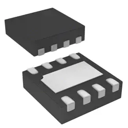
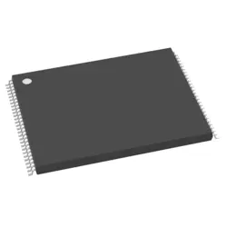
画像は参照用のみです。
GW2A-LV18PG256C8/I7
FPGA - Field Programmable Gate Array
- メーカー
- Mfr。パート #GW2A-LV18PG256C8/I7
- パッケージ
- データシート GW2A-LV18PG256C8/I7 DataSheet
- 在庫中19377
100% オリジナル &新しい
出荷の準備ができている24時間
365日の保証
RFQおよびもっと割引を得る
仕様
| Standard Pack Qty | 90 |
概要
Description
The GW2A-LV18PG256C8/I7 is a specific model of a memory module, likely designed for use in computing applications. It features a capacity of 256 MB, which may indicate it is suited for embedded systems or applications requiring moderate memory support. The "I7" designation could suggest compatibility with Intel's I7 processor architecture or indicate a specific version or variant within the product line.
This memory module may utilize a specific technology or interface, such as DDR (Double Data Rate) SDRAM, to facilitate high-speed data transfer. Its form factor and design would cater to various devices, possibly in industrial, automotive, or consumer electronics sectors.
For detailed specifications, including speed, voltage, and performance characteristics, it's advisable to consult the manufacturer's datasheet or technical documentation related to this model. This will provide comprehensive insights into its applications and compatibility with other hardware.
Features
The GW2A-LV18PG256C8/I7 is a high-performance memory module designed for advanced computing applications. Key features include:
- Capacity: 256GB, allowing for extensive multitasking and efficient handling of large datasets.
- Speed: Operates at high data transfer rates, optimizing performance for demanding workloads.
- Form Factor: Often utilizes DIMM or SO-DIMM configurations, making it suitable for various systems, including servers and workstations.
- Compatibility: Designed to work seamlessly with Intel Core i7 processors, enhancing overall system performance.
- ECC Support: May include Error-Correcting Code (ECC) for increased reliability in critical applications.
- Power Efficiency: Typically operates at lower voltages, reducing power consumption and heat generation.
- Durability: Built to withstand rigorous use, ensuring stability and longevity.
These features make the GW2A-LV18PG256C8/I7 an ideal choice for users looking to upgrade their systems for enhanced speed and performance.
Package
The GW2A-LV18PG256C8/I7 is a package type typically associated with integrated circuits, specifically in a BGA (Ball Grid Array) format. This packaging allows for efficient heat dissipation and compact integration on circuit boards, making it suitable for high-performance applications.
Pinout
The GW2A-LV18PG256C8/I7 is a member of the GW2A family of FPGAs (Field-Programmable Gate Arrays) produced by GOWIN Semiconductor. It features a pin count of 256 pins.
The functions of the pins can vary widely but typically include:
- Input/Output (I/O) pins for interfacing with other devices
- Power supply pins (VCC, GND)
- Configuration and programming pins
- Clock input pins for timing control
- Ground pins for signal integrity
The specific functions of individual pins can be found in the device datasheet, which provides detailed information on pin assignments, electrical characteristics, and functional capabilities.
Manufacturer
The manufacturer of the GW2A-LV18PG256C8/I7 is GOWIN Semiconductor Corp. GOWIN is a semiconductor company that specializes in the design and manufacture of Field Programmable Gate Arrays (FPGAs) and programmable logic devices. Founded in 2014 and headquartered in Beijing, China, the company focuses on providing innovative solutions for a range of applications, including telecommunications, automotive, industrial automation, and consumer electronics. GOWIN aims to deliver flexible and cost-effective FPGA solutions to meet the evolving needs of its customers in various sectors.
Application
The GW2A-LV18PG256C8/I7 is a high-performance, low-voltage FPGA (Field-Programmable Gate Array) primarily used in applications such as telecommunications, industrial automation, automotive systems, and consumer electronics. Its versatility allows for custom logic implementation, signal processing, and real-time data handling, making it suitable for embedded systems, image processing, and control systems in various sectors.
Equivalent
The GW2A-LV18PG256C8/I7 chip is a part of the GOWIN GW2A series. Equivalent products include other GOWIN FPGA variants, such as GW1NR-9C, GW1N-9C, or other GOWIN GW2A devices with similar logic capacity and features. For precise compatibility, cross-reference specifications like pin count, logic elements, memory, and I/O capabilities. Always consult the manufacturer's documentation for detailed comparisons.
出荷
出荷方法私たち
DHL、FedEx、TNT、UPS、またはあなたの選択の他の運送業者を通じてグローバルな出荷サービスを提供します。
出荷料参照(DHL/FedEx):
DHL の: 配送費は25ドル〜45ドル(0.5kg)の範囲で、推定配送時間は2〜5営業日です。
フェデックス: 配送費は25ドル〜40ドル(0.5kg)の範囲で、推定配送時間は3〜7営業日。
UPS の: 配送費は25ドル〜45ドル(0.5kg)の範囲で、推定配送時間は3〜7営業日。
TNT社: 配送費は25ドル〜65ドル(0.5kg)の範囲で、推定配送時間は3〜7営業日。
EMS: 配送料金は30〜50ドル(0.5kg)の範囲で、推定配送時間は7〜15営業日です。
登録航空郵便: 配送費は2〜4ドル(0.1kg)で、推定配送時間は5〜20営業日です。
支払い
Payment Methods
支払い期間は100%前払いです。
現在、下記の支払い方法のみを受け入れています。:
1. ペイパル
2. クレジット・デビットカード
3. ワイヤー 転送
類似
-
![MX25R8035FM1IL0]() MX25R8035FM1IL0
Macronix
-
![MX66U1G45GXDI00]() MX66U1G45GXDI00
Macronix
-
![MX30LF2G28AD-TI]() MX30LF2G28AD-TI
Macronix
-
![MX25L25673GMI-10G]() MX25L25673GMI-10G
Macronix
-
![MX25U25643GZNI00]() MX25U25643GZNI00
Macronix
-
![MX25L2006EM1I-12G]() MX25L2006EM1I-12G
Macronix
-
![MX25U3232FZBI02]() MX25U3232FZBI02
Macronix
-
![MX25L6433FM2I-08G]() MX25L6433FM2I-08G
Macronix
-
![MX25U6435FM2I-10G]() MX25U6435FM2I-10G
Macronix
-
![MX25L12833FZNI-10G]() MX25L12833FZNI-10..
Macronix
-
![MX29LV160DTTI-70G]() MX29LV160DTTI-70G
Macronix
-
![MX25U51245GZ4I00]() MX25U51245GZ4I00
Macronix