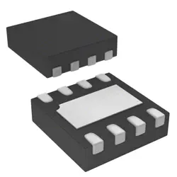
画像は参照用のみです。
GD25Q64ESJGR
IC FLASH 64MBIT SPI/QUAD 8SOP
- メーカー
- Mfr。パート #GD25Q64ESJGR
- パッケージ
- データシート
- 在庫中13577
100% オリジナル &新しい
出荷の準備ができている24時間
365日の保証
RFQおよびもっと割引を得る
仕様
| Series | GD25Q |
| Part Status | Active |
| Base Product Number | GD25Q64 |
| Memory Type | Non-Volatile |
| Memory Format | FLASH |
| Technology | FLASH - NOR (SLC) |
| Memory Size | 64Mbit |
| Memory Organization | 8M x 8 |
| Memory Interface | SPI - Quad I/O |
| Clock Frequency | 133 MHz |
| Write Cycle Time - Word, Page | 140µs, 4ms |
| Voltage - Supply | 2.7V ~ 3.6V |
| Operating Temperature | -40°C ~ 105°C (TA) |
| Mounting Type | Surface Mount |
| Package | 8-SOIC (0.209", 5.30mm Width) |
| Supplier Device Package | 8-SOP |
| Packaging | Tape & Reel (TR) |
| Access Time | 7 ns |
概要
Description
GD25Q64ESJGR is a 64-Mbit serial flash memory from GigaDevice (GD25Q64ES family). It uses an SPI-compatible interface and supports standard SPI, Dual I/O, and Quad I/O read modes with 4-byte addressing for the full memory map. Organization is 8 Mbytes of data with a 256-byte page program, plus sectors (4 KB) and blocks (32 KB/64 KB) for erase; a full-chip erase is available. Features include a status register with write enable, hardware write protection, and deep power-down for low current when idle. Operating voltage is typically 2.7–3.6 V. The suffix “JGR” denotes the specific package/temperature variant (commonly an 8-pin package). Applications include firmware storage and execution-in-place (XIP), boot memory, and external data storage in embedded systems.
Features
Key features of GD25Q64ESJGR:
- 64 Mbit (8 Mbyte) serial flash memory.
- SPI flash with Standard, Dual, and Quad I/O modes; fast read support.
- Operating voltage: typically 2.7–3.6 V; industrial temp range -40°C to 85°C.
- 8-pin SOIC/JGR package (JEDEC SOP-8); RoHS compliant.
- Memory organization: 4 KB sectors; 64 KB blocks; whole-chip erase.
- Page size: 256 bytes; supports standard page program.
- Clock/frequency: up to ~104 MHz read/clock rate.
- Endurance: ~100,000 erase/write cycles per sector; data retention ~20 years.
- Power options: deep power-down mode for low idle current.
- Security and protection: sector/block protection with WP# and status/configuration registers.
- Applications: firmware storage and updates, code flash for microcontrollers, boot ROM, etc.
- 64 Mbit (8 Mbyte) serial flash memory.
- SPI flash with Standard, Dual, and Quad I/O modes; fast read support.
- Operating voltage: typically 2.7–3.6 V; industrial temp range -40°C to 85°C.
- 8-pin SOIC/JGR package (JEDEC SOP-8); RoHS compliant.
- Memory organization: 4 KB sectors; 64 KB blocks; whole-chip erase.
- Page size: 256 bytes; supports standard page program.
- Clock/frequency: up to ~104 MHz read/clock rate.
- Endurance: ~100,000 erase/write cycles per sector; data retention ~20 years.
- Power options: deep power-down mode for low idle current.
- Security and protection: sector/block protection with WP# and status/configuration registers.
- Applications: firmware storage and updates, code flash for microcontrollers, boot ROM, etc.
Package
An 8-pin SOP (SOIC-8) package (RoHS-compliant).
Pinout
- Pin count: 8 pins (SOP-8)
- Function: 64 Mbit SPI serial NOR flash memory (non-volatile storage) with standard SPI interface (CS, CLK, DI, DO) plus WP# and HOLD# pins (VCC/GND).
- Function: 64 Mbit SPI serial NOR flash memory (non-volatile storage) with standard SPI interface (CS, CLK, DI, DO) plus WP# and HOLD# pins (VCC/GND).
Manufacturer
- Manufacturer: GigaDevice Semiconductor Inc.
- Company type: A Chinese fabless semiconductor company that designs and sells flash memory ICs (notably serial NOR/NAND flash) and related memory solutions.
- Company type: A Chinese fabless semiconductor company that designs and sells flash memory ICs (notably serial NOR/NAND flash) and related memory solutions.
Application
GD25Q64ESJGR is a 64‑Mbit serial flash memory used as external non‑volatile storage in embedded systems. Typical applications:
- Firmware storage/boot memory for MCUs/SoCs
- OTA firmware updates and code backups
- Data logging/configuration storage for IoT devices
- Storage for consumer electronics (printers, cameras, set‑top boxes, routers)
- Automotive and industrial control equipment
- Firmware storage/boot memory for MCUs/SoCs
- OTA firmware updates and code backups
- Data logging/configuration storage for IoT devices
- Storage for consumer electronics (printers, cameras, set‑top boxes, routers)
- Automotive and industrial control equipment
Equivalent
Common cross-reference equivalents (64‑Mbit SPI flash, 3.0–3.6 V): Winbond W25Q64FV(W) family; Macronix MX25L6406E; ISSI IS25LP064A; Spansion/Cypress S25FL064K; SST SST25VF064C. These are widely used drop‑in replacements, but verify JEDEC ID, voltage, package, timing and I/O (Dual/Quad) support for your design.
出荷
出荷方法私たち
DHL、FedEx、TNT、UPS、またはあなたの選択の他の運送業者を通じてグローバルな出荷サービスを提供します。
出荷料参照(DHL/FedEx):
DHL の: 配送費は25ドル〜45ドル(0.5kg)の範囲で、推定配送時間は2〜5営業日です。
フェデックス: 配送費は25ドル〜40ドル(0.5kg)の範囲で、推定配送時間は3〜7営業日。
UPS の: 配送費は25ドル〜45ドル(0.5kg)の範囲で、推定配送時間は3〜7営業日。
TNT社: 配送費は25ドル〜65ドル(0.5kg)の範囲で、推定配送時間は3〜7営業日。
EMS: 配送料金は30〜50ドル(0.5kg)の範囲で、推定配送時間は7〜15営業日です。
登録航空郵便: 配送費は2〜4ドル(0.1kg)で、推定配送時間は5〜20営業日です。
支払い
Payment Methods
支払い期間は100%前払いです。
現在、下記の支払い方法のみを受け入れています。:
1. ペイパル
2. クレジット・デビットカード
3. ワイヤー 転送
類似
-
![MX25R8035FM1IL0]() MX25R8035FM1IL0
Macronix
-
![MX25L3233FM1I-08Q]() MX25L3233FM1I-08Q
Macronix
-
![MX25V1635FZNI]() MX25V1635FZNI
Macronix
-
![MX25V2033FM1I]() MX25V2033FM1I
Macronix
-
![MX25R3235FZNIL0]() MX25R3235FZNIL0
Macronix
-
![MX29GL512FHXFI-11G]() MX29GL512FHXFI-11..
Macronix
-
![MX25U51279GXDR00]() MX25U51279GXDR00
Macronix
-
![MX25U3232FZBI02]() MX25U3232FZBI02
Macronix
-
![MX25L12833FM2I-10G]() MX25L12833FM2I-10..
Macronix
-
![MX25U25645GXDI00]() MX25U25645GXDI00
Macronix
-
![MX29F040CQI-70G]() MX29F040CQI-70G
Macronix
-
![MX30LF4G18AC-TI]() MX30LF4G18AC-TI
Macronix