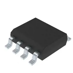
画像は参照用のみです。
FDS2670
MOSFET N-CH 200V 3A 8SOIC
- メーカー
- Mfr。パート #FDS2670
- パッケージ
- データシート FDS2670 DataSheet
- 在庫中5701
100% オリジナル &新しい
出荷の準備ができている24時間
365日の保証
RFQおよびもっと割引を得る
仕様
| Series | PowerTrench® |
| Part Status | Active |
| FET Type | N-Channel |
| Technology | MOSFET (Metal Oxide) |
| Drain to Source Voltage (Vdss) | 200 V |
| Current - Continuous Drain (Id) @ 25°C | 3A (Ta) |
| Drive Voltage (Max Rds On, Min Rds On) | 10V |
| Rds On (Max) @ Id, Vgs | 130mOhm @ 3A, 10V |
| Vgs(th) (Max) @ Id | 4.5V @ 250µA |
| Gate Charge (Qg) (Max) @ Vgs | 43 nC @ 10 V |
| Vgs (Max) | ±20V |
| Input Capacitance (Ciss) (Max) @ Vds | 1228 pF @ 100 V |
| Power Dissipation (Max) | 2.5W (Ta) |
| Operating Temperature | -55°C ~ 150°C (TJ) |
| Mounting Type | Surface Mount |
| Supplier Device Package | 8-SOIC |
| Package / Case | 8-SOIC (0.154", 3.90mm Width) |
| Base Product Number | FDS26 |
概要
Description
FDS2670 is typically a course code associated with a specific subject in the field of food science or nutrition, though the exact content may vary by institution. Generally, an introduction to FDS2670 would cover fundamental concepts related to food safety, food chemistry, and nutritional science. The course might explore topics such as food processing, preservation techniques, and the relationship between diet and health. Students would likely learn about food regulations, quality control, and the impact of food choices on public health. The aim is to provide a foundational understanding of how food affects both individual health and broader societal issues. Practical applications, laboratory work, or case studies may also be included to enhance learning and real-world application.
Features
The FDS2670 is a dual N-channel MOSFET designed for power management applications. Key features include:
1. Low On-Resistance: Provides efficient performance with minimal power loss during operation.
2. High Voltage Rating: Typically rated for a maximum drain-source voltage (V_DS) of around 30V, making it suitable for various applications.
3. Fast Switching Speed: Enables rapid switching, enhancing efficiency in high-frequency applications.
4. Compact Package: Available in a surface-mount package (e.g., SO-8), facilitating easy integration into circuit designs.
5. Thermal Management: Features thermal resistance specifications that help manage heat dissipation during operation.
6. Low Gate Charge: Reduces the power needed for driving the gate, improving overall system efficiency.
7. High Reliability: Designed with robust characteristics to ensure dependable performance in demanding environments.
These features make the FDS2670 suitable for a range of applications, including power supplies, motor drivers, and DC-DC converters.
Package
The FDS2670 is available in a Dual-Flat No-lead (DFN) package, specifically designed for efficient thermal performance and compactness in surface-mount applications.
Pinout
The FDS2670 is a dual N-channel MOSFET with a total of 8 pins. The pin configuration is as follows:
1. Gate 1 (G1) - Controls the first N-channel MOSFET.
2. Source 1 (S1) - Source terminal for the first N-channel MOSFET.
3. Drain 1 (D1) - Drain terminal for the first N-channel MOSFET.
4. Gate 2 (G2) - Controls the second N-channel MOSFET.
5. Source 2 (S2) - Source terminal for the second N-channel MOSFET.
6. Drain 2 (D2) - Drain terminal for the second N-channel MOSFET.
7. Common Source (CS) - Provides a common source connection for both MOSFETs.
8. Internally Connected - Some pins may be internally connected, enhancing thermal performance and ease of use.
The FDS2670 is often used in power management applications due to its low on-resistance and fast switching capabilities.
Manufacturer
The FDS2670 is manufactured by Alpha & Omega Semiconductor Limited (AOS). AOS is a global provider of power semiconductor solutions. The company specializes in the design, development, and supply of discrete and integrated semiconductor devices, primarily focusing on power management products, such as MOSFETs and diodes. Founded in 2000 and headquartered in Sunnyvale, California, AOS operates in various markets, including computing, telecommunications, consumer electronics, and automotive applications. Their products are known for high efficiency and reliability, catering to a wide range of applications in the power electronics sector.
Application
The FDS2670 is a power MOSFET commonly used in various applications, including DC-DC converters, power management systems, battery management, motor control, and power switching in consumer electronics. Its low on-resistance and fast switching capabilities make it suitable for efficient power delivery and thermal management in compact electronic devices.
Equivalent
Equivalent products to the FDS2670 chip include the FDS2671, BSS138, BSS84, and FDS6690. These MOSFETs have similar specifications in terms of voltage, current handling, and package type. Always verify their datasheets for specific requirements and performance characteristics to ensure compatibility in your application.
出荷
出荷方法私たち
DHL、FedEx、TNT、UPS、またはあなたの選択の他の運送業者を通じてグローバルな出荷サービスを提供します。
出荷料参照(DHL/FedEx):
DHL の: 配送費は25ドル〜45ドル(0.5kg)の範囲で、推定配送時間は2〜5営業日です。
フェデックス: 配送費は25ドル〜40ドル(0.5kg)の範囲で、推定配送時間は3〜7営業日。
UPS の: 配送費は25ドル〜45ドル(0.5kg)の範囲で、推定配送時間は3〜7営業日。
TNT社: 配送費は25ドル〜65ドル(0.5kg)の範囲で、推定配送時間は3〜7営業日。
EMS: 配送料金は30〜50ドル(0.5kg)の範囲で、推定配送時間は7〜15営業日です。
登録航空郵便: 配送費は2〜4ドル(0.1kg)で、推定配送時間は5〜20営業日です。
支払い
Payment Methods
支払い期間は100%前払いです。
現在、下記の支払い方法のみを受け入れています。:
1. ペイパル
2. クレジット・デビットカード
3. ワイヤー 転送
類似
-
![MX25L3233FZBI-08Q]() MX25L3233FZBI-08Q
Macronix
-
![MX25V1635FZNI]() MX25V1635FZNI
Macronix
-
![MX25V4035FZUI]() MX25V4035FZUI
Macronix
-
![MX25R3235FZNIL0]() MX25R3235FZNIL0
Macronix
-
![MX25L25673GMI-10G]() MX25L25673GMI-10G
Macronix
-
![MX25L2006EM1I-12G]() MX25L2006EM1I-12G
Macronix
-
![MX25L6433FM2I-08G]() MX25L6433FM2I-08G
Macronix
-
![MX25L12833FZ2I-10G]() MX25L12833FZ2I-10..
Macronix
-
![MX25L25645GXDI-08G]() MX25L25645GXDI-08..
Macronix
-
![MX29F800CBTI-70G]() MX29F800CBTI-70G
Macronix
-
![MX29LV640ETTI-70G]() MX29LV640ETTI-70G
Macronix
-
![MX25V8035FM2I]() MX25V8035FM2I
Macronix