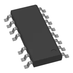
画像は参照用のみです。
FAN48610UC50X
IC REG BOOST 5V 1A 9WLCSP
- メーカー
- Mfr。パート #FAN48610UC50X
- パッケージ
- データシート
- 在庫中4321
100% オリジナル &新しい
出荷の準備ができている24時間
365日の保証
RFQおよびもっと割引を得る
仕様
| Series | TinyBoost® |
| Part Status | Active |
| Base Product Number | FAN48610 |
| Function | Step-Up |
| Output Configuration | Positive |
| Topology | Boost |
| Output Type | Fixed |
| Number of Outputs | 1 |
| Voltage - Input (Min) | 2.5V |
| Voltage - Input (Max) | 4.8V |
| Voltage - Output (Min/Fixed) | 5V |
| Current - Output | 1A (Switch) |
| Frequency - Switching | 2.5MHz |
| Synchronous Rectifier | Yes |
| Operating Temperature | -40°C ~ 85°C (TA) |
| Mounting Type | Surface Mount |
| Package | 9-UFBGA, WLCSP |
| Supplier Device Package | 9-WLCSP (1.22x1.22) |
| Packaging | Cut Tape (CT), Tape & Reel (TR) |
概要
Description
The FAN48610UC50X is a high-performance synchronous step-down converter designed for efficient power management in portable electronic devices. This component is part of ON Semiconductor's line of power management solutions, intended to provide a stable supply voltage even under varying load conditions. Operating at high frequencies, the FAN48610UC50X offers fast transient response and excellent efficiency, making it suitable for battery-operated devices where power conservation is critical.
Key features include a wide input voltage range, low quiescent current, and the ability to deliver up to a specified current output. It typically incorporates advanced protection features such as over-current, short-circuit, and thermal shutdown to ensure reliable operation under challenging conditions. The device is packaged in a compact, thermally efficient form factor, which makes it ideal for space-constrained applications.
The FAN48610UC50X is often used in applications like smartphones, tablets, wearables, and other portable electronics where power efficiency and compact size are paramount. Its design emphasizes ease of integration, allowing designers to implement it with minimal external components, thereby simplifying the overall circuit design.
Features
The FAN48610UC50X is a high-efficiency step-down DC-DC converter. Key features include:
1. Output Voltage: It provides a fixed output voltage of 5.0V.
2. Efficiency: The converter is designed for high efficiency, achieving up to 92% under optimal conditions, which is ideal for battery-powered devices.
3. Input Voltage Range: It operates over a wide input voltage range from 2.5V to 5.5V, accommodating multiple power sources.
4. Load Current: Supports a maximum load current of 1A, suitable for various applications needing moderate power levels.
5. Low Quiescent Current: The device features a low quiescent current, contributing to power savings during no-load conditions.
6. Compact Package: Offered in a compact UCSP package, it’s suitable for space-constrained applications.
7. Protection Features: Includes protection mechanisms like over-temperature, over-current, and under-voltage lockout to ensure operational safety.
8. Soft-Start Functionality: Provides controlled startup to minimize inrush current.
9. Fixed Frequency Operation: Ensures predictable electromagnetic interference performance.
These features make the FAN48610UC50X a versatile choice for portable electronics, optimizing power efficiency and performance in compact designs.
Package
The FAN48610UC50X is in a WLCSP-6 package, which stands for Wafer-Level Chip Scale Package with 6 bumps. This type of package is compact, offering a small footprint ideal for space-constrained applications.
Pinout
The FAN48610UC50X is a high-efficiency, low quiescent current boost regulator developed by ON Semiconductor. It is designed to provide a fixed output voltage of 5.0V. The device is packaged in a small WL-CSP (Wafer-Level Chip-Scale Package) with a pin count of 6.
Here are the pin functions:
1. SW (Switch Node): This pin is connected to the inductor and the internal MOSFET, which is the primary switching node of the boost converter.
2. GND (Ground): This pin serves as the ground reference for the device.
3. VIN (Input Voltage): This pin is used for the supply input voltage range from 1.8V to 5.5V.
4. VOUT (Output Voltage): This pin provides the regulated output voltage.
5. EN (Enable): This pin enables or disables the device. A logic high signal enables the regulator, while a logic low disables it.
6. FB (Feedback): This pin is used for output voltage sensing and regulation.
These functions make the FAN48610UC50X suitable for applications in portable devices where space is limited, and high efficiency is required.
Manufacturer
The FAN48610UC50X is manufactured by onsemi, formerly known as ON Semiconductor. onsemi is a semiconductor company that designs and manufactures a wide range of analog, digital, and mixed-signal integrated circuits. The company focuses on providing energy-efficient solutions for applications in automotive, communications, computing, consumer, industrial, and medical markets.
Application
The FAN48610UC50X is a step-down DC-DC converter designed for applications requiring high efficiency and compact size. It is commonly used in portable electronics, smartphones, tablets, and wearable devices, providing a stable power supply from a battery source. It supports power management in devices where space and power efficiency are critical, offering features like low quiescent current and fast transient response.
Equivalent
The FAN48610UC50X is a high-performance DC-DC buck converter. Equivalent or similar products could include the TPS62085 from Texas Instruments, the LTC3621 from Analog Devices, and the MP2162 from Monolithic Power Systems. It's important to compare specific features, parameters, and pin configurations to ensure compatibility for your application.
出荷
出荷方法私たち
DHL、FedEx、TNT、UPS、またはあなたの選択の他の運送業者を通じてグローバルな出荷サービスを提供します。
出荷料参照(DHL/FedEx):
DHL の: 配送費は25ドル〜45ドル(0.5kg)の範囲で、推定配送時間は2〜5営業日です。
フェデックス: 配送費は25ドル〜40ドル(0.5kg)の範囲で、推定配送時間は3〜7営業日。
UPS の: 配送費は25ドル〜45ドル(0.5kg)の範囲で、推定配送時間は3〜7営業日。
TNT社: 配送費は25ドル〜65ドル(0.5kg)の範囲で、推定配送時間は3〜7営業日。
EMS: 配送料金は30〜50ドル(0.5kg)の範囲で、推定配送時間は7〜15営業日です。
登録航空郵便: 配送費は2〜4ドル(0.1kg)で、推定配送時間は5〜20営業日です。
支払い
Payment Methods
支払い期間は100%前払いです。
現在、下記の支払い方法のみを受け入れています。:
1. ペイパル
2. クレジット・デビットカード
3. ワイヤー 転送
類似
-
![MX25V1635FZNQ03]() MX25V1635FZNQ03
Macronix
-
![MX66U1G45GXDI00]() MX66U1G45GXDI00
Macronix
-
![MX25V5126FM1I]() MX25V5126FM1I
Macronix
-
![MX25V2033FM1I]() MX25V2033FM1I
Macronix
-
![MX25V16066M2I02]() MX25V16066M2I02
Macronix
-
![MX25L6433FM2I-08G]() MX25L6433FM2I-08G
Macronix
-
![MX25U6435FM2I-10G]() MX25U6435FM2I-10G
Macronix
-
![MX25L12833FZNI-10G]() MX25L12833FZNI-10..
Macronix
-
![MX29F040CQI-70G]() MX29F040CQI-70G
Macronix
-
![MX25L25735FMI-10G]() MX25L25735FMI-10G
Macronix
-
![MX25L1006EMI-10G]() MX25L1006EMI-10G
Macronix
-
![MX25R4035FM1IL0]() MX25R4035FM1IL0
Macronix